
This design and implementation was conceived as a joint project between CERN [1] and the INFN [2] with the following aims in mind:
The architecture and circuit design was shared between CERN and INFN, the
printed circuit layout was done at CERN and the printed circuit fabrication
was subcontracted out to a third party manufacturer.
Ten DSNIC boards have been in constant exploitation since late 1996 and
have no known bugs.
The architecture is shown in Fig 1.
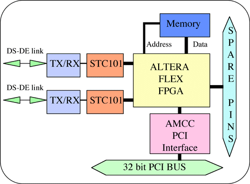
The design goal was first to provide host control to the platform through some known interface chip (for security) and secondly to provide outputs in the form of one or two DS links. For simplicity there would be no embedded processor. All the intelligence, control, and `glue' functionality would be subsumed into one large programmable gate array. This approach provided for maximum flexibility with the possibility of maximum hardware performance provided that the resources could be sufficiently exploited. It also ensured a simple design and minimised design and development risk . The functionality and performance of the platform is therefore totally under the control, and limits, of the firmware loaded into the FPGA.
A commodity interface chip, the AMCC 5933 provides the necessary PCI
master, slave, DMA, interrupt and mailbox facilities between the onboard
resources and any PCI bus host.
Details of the AMCC chip can be found at http://www.amcc.com/Products/PCI/S5933.htm
All the `user-side' data and control lines are handled by logic implemented
in the FPGA.
There are optionally two interfaces to DS links using the STC101 Parallel
to Serial link drivers. Details of the chip can be found at http://www.hensa.ac.uk/parallel/vendors/inmos/ieee-hic/data/C101-04.ps.gz
The appropriate differential transceivers and common-mode rejection chokes
are incorporated on-board to provide a secure physical layer for data transmission.
Access to the STC101's is entirely controlled from logic implemented in
the FPGA.
A bank of 128Kbyte of SRAM is optionally available and configured as byte writeable, byte readable 64 bits wide by 16Kwords deep. Access to the memory is entirely controlled from logic implemented in the FPGA.
All the onboard resources are controlled from the Altera FLEX 10K50
family in PGA packaging. Details of the chip specifications can be found
at http://www.Altera.com/html/products/f10k.html
There is sufficient board space to permit the mounting of a ZIF socket
for easy speed upgrades. The FPGA can be optionally intialised from:
The PCI interface runs at 33Mhz from the bus PCI _CLK. The STC101 link engines are clocked at a nominal 50MHZ to achieve 100Mbits/sec. The STC101 parallel interface is clocked at PCI_CLK/2=16.5 Mhz. The FPGA logic runs under the two clock domains of 33 and 16.5 Mhz.
There are separate serial memories to initialise the BIOS variables of the PCI interface and the initial conditions of the Altera FPGA.
The FPGA has 24 spare pins if both STC101's are mounted and 81 spare pins if the second STC101 is not mounted. All these spare pins are brought out to headers for exploitation in the patch area of user defined functionality.
Each STC101 produces a DS link which is brought out to the front panel HARLINK connectors. In addition there are HARLINK connectors for Host Reset and Target Reset permitting the board to be used as either as a Reset daisy chain host or as one of the targets along the Reset chain.
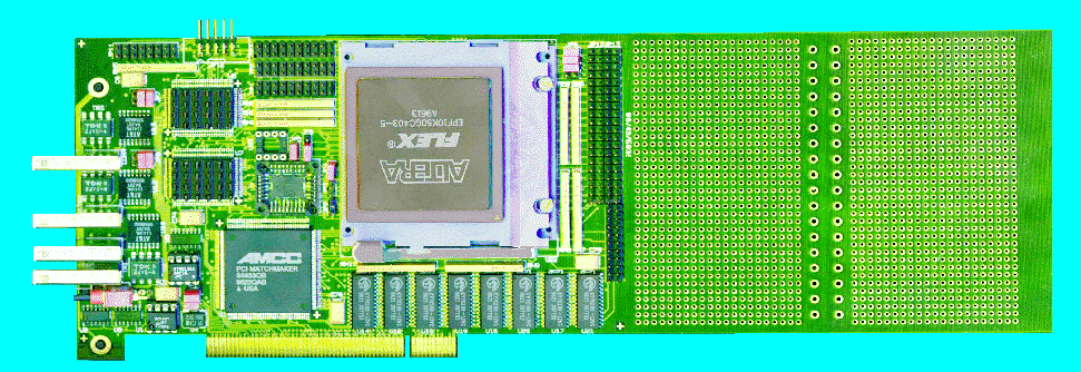
The electronics are mounted on a full length PCI form factor board.
Users should be aware that on some PC compatible motherboards this restricts
the freedom of choice of available PCI slots since the long board may be
in conflict with motherboard elements such as heatsinks, fans, memory subsystems
etc.
A picture of the mounted and working board (minus the front panel) is shown
in Fig 2.
[1] European Laboratory for Particle Physics .
http://www.cern.ch/ and http://www.cern.ch/HSI/dshs/
[2] INFN Rome :
http://www.roma1.infn.it/ and http://mulflx.roma1.infn.it/atlas/rmwork/lvl2muon.html
1) A4 version of poster " The Network Interface Bottleneck http://www.cern.ch/HSI/dshs/marcel/marcel.ps (Postscript file - 2.2 Mbytes)", or http://www.cern.ch/HSI/dshs/marcel/marcel.ps.gz gzipped Postscript (900 kbyte), presented at RT 97, Beaune, 22-26th September, 1997.