
DSNIC: Brief Firmware Description.
Marcel Boosten
CERN, EP/ATD, Geneva, Switzerland
December 12 1997
Table of Contents
Introduction
The DSNIC firmware has been designed to full fill two requirements:
-
It should provide network access to the DS link control network to
allow a PCI based system to be the DS network controller.
-
It should support a high speed message passing protocol.
The DSNIC card contains two C101 DS link interfaces. The first C101
is used to provide register I/O based network access meant for
network control. The second C101 is used to support the high speed
message communication protocol.
We have designed a high speed message passing protocol with the
following characteristics:
-
To avoid long term blocking of a wormhole route, the protocol should
split messages into packets.
-
The protocol should support adaptive routing because adaptive
routing has advantages for both throughput and reliability. The
consequences of supporting adaptive routing is out-of-order packet
delivery. The protocol should therefore reorder packets on the
receiving side.
-
To avoid network congestion, the message receiver should be capable
of receiving data as soon as it is offered. Since the buffering
capabilities of each end-node are limited, the protocol uses
end-to-end flow control to avoid packet loss due to buffer overflow.
Firmware design
The design of the firmware is the result of the following arguments:
-
Packet communication interface:
Measurements have proven that the maximum link throughput cannot be
reached if the host CPU is used to transfer every single byte of a
message via register I/O. Therefore, the DSNIC firmware offers an
packet communication interface that allows DMA transfers of packet
data.
-
DMA to user space:
A well known problem in interfacing is memory-to-memory copying.
Memory-to-memory copying is an expensive and non-essential operation
which causes both CPU loading and latency. To avoid packet
reordering to be an expensive operation, the software should be
capable to determine on basis of the packet header where the packet
data is to be stored via DMA to user space. The firmware supports
this by splitting packet header from packet data and generating
interrupts on header reception.
-
Low latency acknowledges:
Due to end-to-end flow control is the latency of acknowledge packets
critical for the message latency. The firmware improves the
acknowledge latency by offering two separate outgoing FIFOs for
acknowledge and data packets, which allows acknowledges to pass by
data packets.
-
Support different packet sizes:
The packet size determinates the number of packets that need to be
handled by the host CPU, and it therefore strongly influences the
CPU load. To investigate this influence, the firmware supports
packet sizes of 2 to the power n, where 2 < n < 13.
-
Maximise throughput:
To allow maximum throughput communication, the firmware should hide
the latency of the controlling software. The firmware does this by
providing data buffering via FIFOs.
Architecture
Figure 1 shows a block diagram of the firmware. The functions are
described in AHDL and compiled to run on the -3 version of the
Altera 10K50.
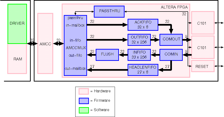
Figure 1: AHDL functional block diagram.
Detailed design
COMIN takes care of packet reception, it splits packet headers from
packet data. The headers are send to the HEADLENFIFO, and the data
is send to the INFIFO. Apart from splitting, COMIN also counts the
packet length, which is known as soon as the end-of-packet character
has been received. Also this length is send to the HEADLENFIFO.
Data in the HEADLENFIFO is delivered to an AMCC mailbox, which can
generate an interrupt. On a header reception interrupt, the host CPU
can establish the receiving DMA.
COMOUT takes care of sending data and acknowledge packets. If data
is available in both the ACKFIFO and the OUTFIFO, data in the
ACKFIFO will be selected. This way, acknowledges can pass by
enqueued data packets.
In order to hide the latency of the controlling software, there are
FIFOs on both the receiving and the transmitting side. The buffer
size of 1 Kbyte was chosen as a good fit into the internal resources
of the Altera FPGA and it can hide a latency up to 100 usec which
should be sufficient to hide software latency.
To avoid a store-and-forward system, the receiving DMA must be
initialised as soon as the header of the packet is
received. However, the length of the DMA transfer should be known
beforehand. This is not the case, since the packet length is
determined by COMIN via counting. Therefore FLUSH pads out each
packet to the full packet length. DMAs can now be set up immediately
on header reception, using the full packet length.
AMCCMUX multiplexes the AMCC to all the FIFOs. PASSTHRU provides
access to the registers of the C101 and the reset links.
Resource usage
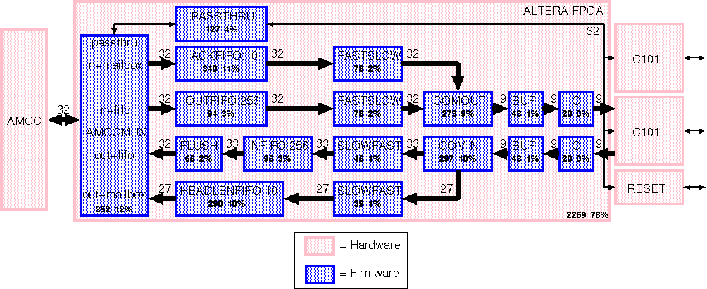
Figure 2: Resource usage of the firmware.
Figure 2 shows the FPGA resource usage. The Altera 10K50 contains a
total of 2880 Logic Cells (LCs). Due to limitations in logic
placement, only about 80% of these resources can actually be
used. Upto 20% of the LCs in the firmware can be made available for
additional purposes by reducing the size of the ACKFIFO and the
HEADLENFIFO. Currently, these FIFOs are maximised to just fill the
Altera 10K50.
Figure 2 contains more functional blocks than Figure 1. The extra
blocks FASTSLOW and SLOWFAST take care of data transfer from one
clock domain to the other. Furthermore, there are IO and BUF blocks
which ensure the timing constraints with respect to the C101
interface.
Performance
Figure 3 shows the throughput versus message length for
bidirectional message exchange (Comm2) and for some different packet
sizes (8, 1024, and 4096). The results show the end-to-end data
bandwidth between two Linux processes. Each process is running on a
200 MHz Pentium PC.
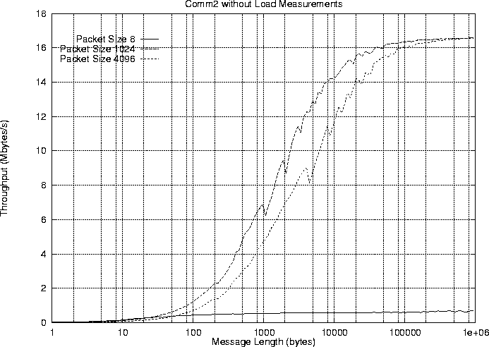
Figure 3:
Bidirectional throughput versus message length for different packet
sizes.
This graph proves that the DSNIC can reach a bidirectional
process-to-process throughput of 16.6 Mbytes/s, which is 90% of the
theoretical bandwidth.