PLD IRRADIATION TEST PROJECT
The aim of this project is to develop a circuit board in order to test
a candidate programmable logic device (PLD) for implementing a radiation
tolerant S-LINK source card
(LSC). This board can be used as a simplex S-LINK Link Source Card that
is using G-LINK as physical layer, or as a data generator test card for
radiation testing. The actual function depends on the configuration
of the FPGA.
If the FPGA is configured for data generator, two independent data paths
can be used to check the correct functioning of the card. At this configuration
the card requires three control signals on its differential (RS-422) inputs
which select test patterns or reset the card. Four different data
patterns can be selected by the control signals. The FPGA generates
"Test Pulses" on four differential lines, which monitor the internal functioning
of the digital logic. These four signals are transmitted to a data analyzer
via an RS-422 Line Driver and twisted pair cable connections.
The second data path serves for monitoring the joint functioning of
the FPGA, Serializer and Media Interface. Test pattern generated
by the FPGA is framed into 224+2 word packets which start and terminate
with a control word. The four MSB of the data words contain parity bits
for each four bits respectively. The serialized data is transmitted
using optical (any standard 9 pin) or electrical (Lemo connector) media
interface.
In case the FPGA is configured for S-Link Source, the card serializes
and transmits the data which is sent to its S-LINK connector via electrical
or optical media . The simplex G-LINK
LDC can be used as receiver.
Single Event Effect and Total Dose tests will investigate the adequacy
of the selected devices for the ATLAS
Front-End links. Expected error rate will be established for the different
Front-End link environments.
Radiation Test Setup
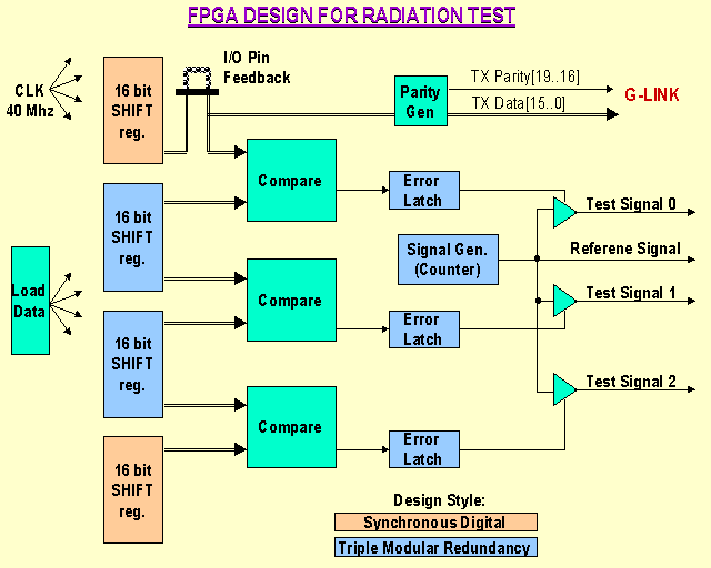
FPGA Design Block Diagram
Different test patterns can be generated by the loadable circular shift
registers (walking 1, walking 0, alternating bits, walking FF). This data
is sent to the G-Link serializer. To test the internal functioning of the
PLD, four shift registers are implemented, two with triple modular redundancy
which reduces the single event upset probablity and two using single flip-flops.
One data path is sent to and fed-back from device pins to test the I/O
circuits as well. The data patterns at the outputs of the shift registers
are compared in each clock cycle. If no errors have occurred, the comparison
result will be true. If a SEU (Single Event Upset) occurs in one
of the shift registers, in the I/O feedback path or in the comparator,
the result of the comparison will be false. Since the signaling speed is
limited on the twisted pairs going to the control room, multiple words
are compared in one "test period" and a latch will be toggled if one or
more comparison errors occur during this time. The length of a test period
is 6.4us. At the end of each test period a "control pulse" is sent from
a counter on one twisted pair. Similar, "test" pulses are generated on
the 3 other twisted pairs in case no comparison errors occurred during
the test period. The theoretical error probability (the probability that
the pulse is missing at the end of a test period) is different on each
line. The shift registers are reloaded at the beginning of each test period.
This method ensures a slow signaling rate on the twisted pairs and full
speed operation of the internal logic circuits. All logic circuits are
synchronous, the clock frequency is 40Mhz which is the read-out frequency
of most ATLAS Front-End links. SEU mitigation methods should be used to
implement the control pulse generating circuits.
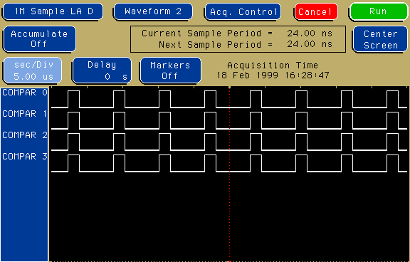
Test pulses are sent to the control room
A Line Receiver will send the received pulses to a PC via a National
Instruments PCI-DIO-32-HS high speed digital I/O module. Data acquisition
and error detection is controlled from Labview. The error detection can
detect if one or more (control or test) pulse is missing or if non of the
pulses are received, as control pulses will arrive periodically. If the
control pulse is missing, it is due to an error occured in the pulse generator
circuit. In case no pulses are received for a longer period, permanent
damage of the circuit is probable. In this case manual intervention (system
reset or power down) is necessary.
(Re)Started with pattern 1010101010 06/04/08:38:46
23295.88 3
(Re)Started with pattern 1010101010 07/04/08:39:47
(Re)Started with pattern 1010101010 07/04/08:45:47
(Re)Started with pattern Walking One 07/04/08:47:16
15490.25 3
15633.71 C
19069.58 C
3
44502.39 3
56896.82 E
59727.74 8
7
60010.22 8
|
Example of an error log file generated with Labview:
Test pattern, Start time, Error type and Time stamps in seconds
relative to start time are recorded
The G-LINK serialiser (HDMP-1022) sends serial data to the optical media
interface. At the receiving side the simplex G-LINK
LDC will be used. The FPGA of this card includes an automatic data
checker, so this card will check the data pattern, parity and packet length
of the received packets. In case of mismatch, an error code is generated
and the erroneous data with the error code will be written into the host
computer (PC, Linux).
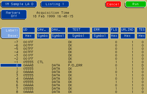
The LDC checks the received data and sends the error code (TEST
tag on the picture) to the Logic Analyzer
On this picture the analyzer triggered on a Parity and Data comparison
Error
Radiation Environment
TCC2
This card will be first irradiated in the TCC2
area of the SPS accelerator. The estimated dose rate is about 50 Gy
and 5.1010 neutrons/cm-2 which can be accumulated in a 6 week running period
of SPS. In one year depending on how the accelerators are operating,
this gives 3x10**11 neutrons cm-2. The dose rate is monitored on-line at
7
locations of the test-area. The card is mounted on a SLITEST board
and inserted into a VME crate close to PMITC03 and PMITC04 dosimeters.
Dose measurements can be found here.
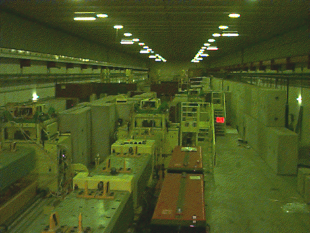
The TTC2 area, looking along the beams
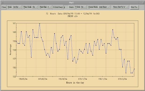
On-Line Radiation Monitor Display
PSI
We irradiated the FPGA on this card at Paul
Scherrer Institute, in a focused proton
beam which is originally used for medical purpose. This beam is a ~64
MeV proton beam at 1.25E9 p/cm^2/s. It corresponds to an 0.5 MRad /h dose
rate or 1E13 n/cm^2/h (1MeV) neutron fluence.
Circuit Board Description
The board is powered through the S-Link connector. The ACTEL
A54SX16 FPGA generates test data for G-Link, and test signals for monitoring
the FPGA only. G-Link data is serialised by the HDMP-1022 G-Link transmitter
chip. Serial data is sent to the Methode
19-4-1-S (Multimode, 850nm) laser driver. The FPGA-test signals from
the FPGA are sent to the HS-26C31RH radiation
hard Line Driver which transmits the data to the control room via 4
twisted pairs. The HS-26C32RH radiation
hard Line Receiver receives control signals (reset, pattern select)
from the control room. A TEMEC
QEN47CHRAY100SB 40 Mhz quartz oscillator is used as system clock
source, the 3.3V FPGA is powered by a LM117H
linear regulator.
All signals of the S-Link connector are connected to I/O pins of the
Actel chip so with a proper FPGA configuration this board can be used as
a G-LINK based S-Link source card, which can transmit 16 or 32 bit words
at max. 150 Mbyte/s.
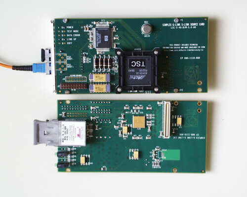
G-Link - S-Link Source Card for Radiation Tests
Main Components
FPGA: ACTEL A54SX16
Quartz Oscillator: TEMEX
QEN series (or VECTRON
M55310 series)
Voltage Regulator: (for 5V -> 3.3V conversion) LM117HTotal
Dose Test Results SEL
test results
As this chip did not fulfil our requirements, we are planning
to test the HS-117RH
regulator.
Serializer: HDMP
- 1022 (HP - G-Link Transmitter) Radiation
Testing Results
Media interface: Methode MDX-19-4-1-S Radiation
Testing Results
RS-422 Line Driver/Receiver: HS-26C31RH
/ HS-26C32RH
Power Filtering Capacitors: 470nF, ceramic
Results (Preliminary)
-
On the first two weeks the card was powered from the power supply of a
VME Crate. A power MOSFET transistor was found to be extreamly sensitive
to radiation in the VME's power supply and three power supply units have
died in a very short period, after a few Grays of radiation.
-
The power supply was changed to an external one which is placed to an area
where the dose rate is relatively low.
-
The total accumuted dose between 5th of April and 7th of June is ~ 5Krad.
The card stopped functioning on the 7th of July at 21:21. The problem was
the degradation of the LM117H
Linear Regulator chip which generates 3.3V supply voltage from 5V for the
Actel chip. Its output voltage has dropped to 25% of its before irradiation
value. The chip was replaced on the 29th. of July.
-
Both bit upsets and synchronisation errors were observed on the datalink.
As the FPGA did not have any SEUs these errors were caused by the serialiser
or the laser driver. The upset rate was in correlation with the changing
dose rate. The most errors were measured on the 3rd. of July: 160 bit flips
and 21 loss of synchronisation. The average error rate between the 3rd
of June and the 7th of July is 10-20 bit flips and 1-4 synchronisation
errors per day.
-
No errors were observed on the A54SX16 FPGA.
-
The Actel chip also survived a 90 minutes irradiation period at PSI
(750Krad!) and no single events were observed. These results are to be
verified as this chip did not survive so high total dose at NASA-GSFC.->
-
The Actel chip (An A54SX16 from the same order) was irradiated by Rich
Katz at NASA-GSFC with a Co-60 source, the dose rate was appr. 1 krad(Si)/hour.
TEST
RESULTS
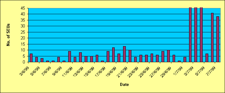
Number of detected Single Event Upsets from 3/6 to 7/7 1999
Future plans to make
a radiation hard Gigabit datlink card
As technology advances the supply voltage of the digital chips is decreasing.
At the design of this board we could not avoid using circuits with different
supply voltages (5V and 3.3V) on the same board, generating the lower supply
voltage with a voltage regulator. As 2.5 supply voltage chips will also
appear in the future we probable will be able to eliminate the use of a
voltage regulator. The present LM117H
chip proved to be rather sensitive to radiation. We are planning to radiation
test the HS-117RH
radiation hardened voltage regulator.
It is necessary to find a radiation tolerand serialiser which does not
loose synchronisation in radiation since thousands of datawords are lost
while the link regains synchronisation.
Future investigations are necessary to prove the radiation tolerance
of the Media Interface.
Last updated: 25.11.1999
Any comments, questions and critics are welcome!
Zoltán
Meggyesi
CERN / KFKI-RMKI