The GOL is basically a simple 20-bit serialiser with an integrated PLL. It nominally inputs the 20-bits data at a rate of 60 MHz and sends it out at a baudrate of 1.2 GHz. The 60 MHz clock is generated out of a 40 MHz clock which is input to the GOL. The GOL chip is designed to test the high-speed critical parts (PLL, serialiser) that are needed to make a fully usable serialiser chip. A complete serialiser chip will also contain a coding scheme to keep the DC balance, a VcSEL driver and some low speed protocol logic. The GOL is made in deep submicron technology using design techniques that make it resistant to radiation effects.
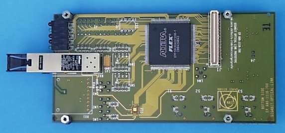
The GOLPROTO printed circuit board contains an Altera 10K30A FPGA which is able to send different data patterns and which can send the serial configuration stream to the GOL. The GOL chip is bond wired on the PCB. In a second phase it may be possible to use the GOLPROTO as an S-LINK Link Source Card as an S-LINK connector is integrated on the card with its signals connected to the Altera.
The card is not commercially available.
| 12 March 1999 | First meeting |
| 7 May 1999 | Received pinout of GOL chip |
| 20 May 1999 | GOL chip submitted for fabrication. Expect unpackaged samples to return 31 July 1999 |
| 11 June 1999 | Design review of schematics |
| 23 June 1999 | Final version of schematics, components being ordered, PCB design started |
| 19 July 1999 | PCB design finished. Ordered 5 PCBs (produced at CERN) |
| 2 August 1999 | PCBs arrived. Three boards will be mounted |
| 7 September 1999 | Three boards mounted, Altera programs tested (without GOL chip) |
| 13 September 1999 | GOL chip production had problems. New batch should be ready by mid October |
| 20 September 1999 | GOL presented at LEB99, Fifth Workshop on Electronics for the LHC Experiments |
| 11 October 1999 | Chips received |
| 15 October 1999 | Chips working. Eye diagram looks great. Data transmitted optically (via 9-pin and via SFF transceiver) to HP G-LINK receiver |
| November 1999 | Radiation tests made |
| 9 December 1999 | Results presented at the 5th RD49 workshop |
| 8 January 2001 | GOL chip submitted. Version with protocol and coding engines integrated |
| 13 March 2001 | GOL chip with protocol engines being tested |
| 11 June 1999 | Altera design started. Written in Verilog language |
| 7 September 1999 | Altera design tested. |
CERN - High
Speed Interconnect - S-LINK
Erik van der Bij - 13 March
2001