

ODIN S-LINK Hardware Specification
Introduction
This document is intended as a designers note on the ODIN S-LINK interface
and is for anyone who has to understand the internal functions of
ODIN, or for anyone who wants to know more details than the ODIN data sheet
features. The reader should have a profound knowledge
Features
Main Features
-
Duplex version - D
-
Max. 40 MHz User Clock (UCLK) - 40
-
Block basis error reporting - B
-
5.0V or 3.3 V supply voltage - 5.0/3.3
-
Maximum 160Mbytes/s - 160
-
S-LINK code - LSC/LDC-D-40-B-5.0/3.3-160
Single version features
-
32 MHz link clock
-
128 Mbyte/s maximum data rate
-
64 Mbytes/s maximum control word rate
-
8 MHz return line sampling
Double version features
-
40 MHz link clock
-
160 Mbyte/s data rate
-
80 Mbytes/s maximum control word rate
-
5 MHz return line sampling
Additional features
-
Improved reset protocol
-
32 bit data width only
Forward Channel
The low power G-Link is run from an on-board oscillator since the receiver
chip needs a reference clock for locking onto serial data stream. The G-Link
features 17-bit parallel input, including flag bit. It also features a
possibility to send a 14-bit control word. This section describes how the
33-bit S-LINK protocol is mapped to the 17-bit G-Link protocol. It also
describes the internal commands the ODIN LSC and ODIN LDC use for communication.
Data Words
The G-Link protocol is defined on a word-basis only. Therefor there is
no need to pack the data into frames when transfering and to reduce loss
of bandwidth no extra framing protocol other than what the S-LINK control
words specifies is used.
The 32-bit S-LINK data word is sent as two consecutive 16 bit G-LINK
words. Flag bit is high for data words and no other
odd/even word indicator is used. The most significant bits, LD[31..16],
are sent first, followed by least significant bits, LD[15..0], on the next
clock cyle. No idle words between msb and lsb are allowed. Idles between
S-LINK words are allowed but not necessary.
See below for transmission exampel including
control words and CRC
Data demultiplexing
In the Double ODIN version, two G-Links are used in the forward channel.
The data splitting protocol is decribed in figure 1
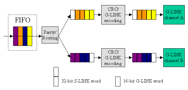 Figure 1. Data splitting in double G-LINK version
S-LINK data is written into the FIFO (left 2x4 block) at positive edge
of UCLK, typically 40 MHz. The routing logic reads from the FIFO at positive
edge of XCLK, the on-board oscillator, 40MHz.. As there is no framing
it is important that not only upper and lower half of each word is sent
in a defined order, but also that data from the A and B channels that are
sent the same cycle also arrives at the LDC the same cycle. The cable length
difference must be small to meet this requirement. The B channel receiver
in the double G-Link version is in PASS-mode, see HDMP-1032/34 for details,
and this introduces an extra latency of 0.4 cycles, equivalent to ~2 meters
of optical fiber. If cable lengths are different the B-channel should have
the shorter cable.
In the single G-LINK configuration, only the A-channel (upper) is available,
and the routing logic uses the 64 MHz on-board oscillator, reading at every
other cycle. In this mode, data is written to the G-LINK at 64 MHz. On
the single ODIN LDC the 64MHz receiver clock must me frequency divided
to 32 MHz to meet S-LINK rquirements of maximum 40 MHz LCLK.
CRC
CRC - Cyclic redundancy code.
CRCC - Cyclic redundany code checksum, 16 bit cheksum appended to data
stream.
The 16 bit CRC-CCITT i.e. the polynomial X16+X12+X5+1,
is used as error detection for data words. A CRCC is sent in the following
cases:
-
Before a control word, if data has been transmitted.
-
After average 1024 S-LINK dataword (4kB) of data per channel.
Note that a CRCC is not be sent when the LSC fifo is empty. When UCLK is
sligthly below 40 MHZ, or 32 MHz in single G-LINK configuration, this would
cause a dramatic decraese i over all speed as seen in previous S-LINK implementations.
A CRCC is always sent over both channels and will always be preceeded
by a CRCC command. The error signal on the control
words is ORed from the error signals from both channels, and the
individual error signals are shown on LD[3..2] for diagnostic reasons.
Since there is no begin-CRC-stream it is important that the CRC works in
a similar manner on both cards. The CRC should be reset on RESET commands
and CRC commands sent over the forward channel. When resetting a CRC the
quotient can be set to arbitrary values and the the ODIN link the value
of all ones is chosen for simplicity and the ability to count commencing
zeroes, which a CRC preset with all zeroes does not have. It is common
practice to reset CRC quotient to '1'.
Since the error detection is only visible in control words, every transmission
of data should be ended with a control word, and a CRC checksum is
sent and CRC logic on both cards are reset. Figure 2 shows an example when
a data block of 4-8kB of data is sent over one channel, followed by a controlo
word.
4kB
data |
CRC
Command |
CRCC |
<4kB
data |
CRC
Command |
CRCC |
Control Word |
Figure 2. Transmission example with CRC
Control Words
An S-LINK control word (28-bit word) is sent as a 2 G-LINK data words with
flag bit low for both cycles. If data have been sent since last control
word, a CRC checksum is sent over all available channels.
Even parity i used as error detection for control words. Even parity
is chosen so that a control word containing all zeros (for example in test
mode) will have all parity bits also zero. Since control word is sent as
2 G-Link data words, 4 unused bits are available. These are LD[3..0] and
these are
| LD[31..4] |
LD[3] |
LD[2] |
LD[1] |
LD[0] |
| Control Word |
Even parity bit for LD[31..25] |
Even parity bit for LD[24..18] |
Even parity bit for LD[17..11] |
Even parity bit for LD[10..4] |
Figure 3. Control Word with parity bits
The control word, including the parity bits, are now sent in the same
manner as data word, with LD[31..16] followed by LD[15..4]+parity
the next cycle.
At LDC, parity bits are checked, and according to S-LINK specification,
these lowest four bits are reserved for error detection report.
Command Words
Internal S-LINK commands are sent as G-LINK control words. The control
bits have the following meaning: (bit 14 and 15 used internally by the
G-LINK). If an error is detected in any bit, the LDC should disregard the
word. Rx[13..10] are reserved for future use and current receiver disregards
these bits.
|
Rx[9..0]
|
Symbol
|
Command
|
|
"0000000011"
|
CRCC
|
Next word a CRCC
|
|
"0000001100"
|
TON
|
Test mode on
|
|
"0000110000"
|
TOFF
|
Test mode off
|
|
"0011000000"
|
RLDWN
|
LSC down
|
|
"1100000000"
|
RRES
|
Remote reset
|
Figure 5. Internal ODIN commands
G-LINK Flag bit
The G-LINK flag bit is used to distinguish between control word and data
word. For data words flag bit is high during transmission, and for control
words flag bit is low. For CRC the flag bit is high during the transmission
of the CRCC, so flag bit also indicates that the received word is a part
of the CRC data stream.
| Transmission |
TX_DATA |
TX_CNTL |
TX_FLAG
|
| Data word |
high
|
low
|
high
|
| Control word |
high
|
low
|
low
|
| ODIN Command |
low
|
high
|
n/a
|
| CRC checksum |
high
|
low
|
high
|
Figure 6. Overview of G-LINK control bits.
Test mode
The ODIN uses the standard S-LINK test pattern, the walking bit pattern.
The test mode is started by sending a 'test-mode-on' command and ended
with a 'test-mode-off' . The return channel is working as normal in test
mode. Each test mode cycle is commenced by a test-mode-on command
Transmission example
Here is a longer transmission exampel for doubel channel version. For single
channel version the main difference is that only one CRC is sent. The example
contains the following data:
-
Beginning of fragment Control word, CW1
-
4 S-LINK Data Words DW1-DW4
-
2 CRC command+CRCC, one per channel
-
End of fragment Control word, CW2
Channel A
| TX/RX[15..0] |
FLAG |
DATA |
CNTL |
| CW1[31..16] |
0 |
1 |
0 |
| CW2[15..4]+par[3..0] |
0 |
1 |
0 |
| DW2[31..16] |
1 |
1 |
0 |
| DW2[15..0] |
1 |
1 |
0 |
| DW4[31..16] |
1 |
1 |
0 |
| DW4[15..0] |
1 |
1 |
0 |
| CRC command |
- |
0 |
1 |
| CRCC |
1 |
1 |
0 |
| x |
x |
x |
x |
|
Channel B
| TX/RX[15..0] |
FLAG |
DATA |
CNTL |
| x |
x |
x |
x |
| DW1[31..16] |
1 |
1 |
0 |
| DW1[15..0] |
1 |
1 |
0 |
| DW3[31..16] |
1 |
1 |
0 |
| DW3[15..0] |
1 |
1 |
0 |
| CRC command |
- |
0 |
1 |
| CRCC |
1 |
1 |
0 |
| CW1[31..16] |
0 |
1 |
0 |
| CW2[15..4]+par[3..0] |
0 |
1 |
0 |
|
Figure 7. Longer transmission example
Return Channel
The return channel also uses a G-LINK as physical layer. All words are
sent as data word, no flag bit used. For error detection every bit is sent
twice. If an error is detected in the word the word is discarded. No flag
bit or control word is used.
| Bits |
When "11" |
| [1..0] |
RL[0] high |
| [3..2] |
RL[1] high |
| [5..4] |
RL[2] high |
| [7..6] |
RL[3] high |
| [9..8] |
Flow control, XOFF |
| [11..10] |
LDC down |
| [13..12] |
Remote reset |
| [15..14] |
Reserved |
Figure 8. Return channel data and commands
Reset protocol
The reset protocol is changed from the S-LINK specified card reset
to a link reset. When either side detects a problem with the link,
ie the receiver(s) do not aquire lock on serial data, a link down command
is sent to the other card, making it go down. If URESET# is set low on
either side, a Remote reset command (RRC) is sent to the other side, making
both cards go up when the error is cleared.
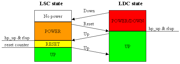
LSC Power-up and Reset State machine
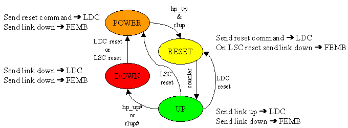
LSC powers up in POWER state. From there it waits for a hp_up, 21-bit
filter signal on Transmitter locked and Receiver ready signal, and rlup,
indicating that a command other than link down is received on return channel.
Counter in RESET-UP transition is reset after a LSC reset and assures link
down to be 4 clock cycles at a LSC reset.
When link is up and LDC is reset, LSC goes into RESET state to answer
reset command. This is necessary since CRC and LDC is reset only on this
LSC reset command. When answering reset command the reset counter is not
started, and LSC will stay up during LDC initaiated reset cycle.
In POWER and DOWN state, 1 command word is sent followed by 7 idles.
This is to make LDC G-Link receivers to aquire faster and more secure lock,
as it prevents improper word alignment caused by static valid code field
embedded within the data field that the command words have..
LDC Power-up and Reset state machine
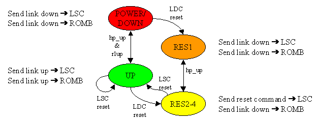
LDC powers up in POWER/DOWN state. Here the LDC waits for hp_up and
rlup, and is continuosly sending link down command to LSC. By doing this,
it is assured that LDC will come up before LSC in power up sequence, and
no data written to LSC will be lost. When LDC is in UP state, a LSC reset
will do nothing to the state machine, but CRC error latches and Test mode
state is cleared.
Return channel always send 1 word followed by 7 idles to make LSC G-Link
receiver to aquire faster and more secure lock.
Power-up sequence, LSC powered up first
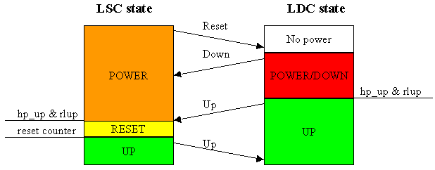
Power-up sequence, LDC powered up first
Clock domains
LSC
LSC has three more or less independant clock domains. UCLK is the
user clock, maximum 40MHz,and this is decoupled from the internal logic
thorugh the asynchronous FIFO. However, at LSC reset a counter is run from
this clock to assure 4 cycles of LDOWN# low, which is specified in the
S-LINK spec. XCLK is the transmission clock from most of the LSC
logic runs from. RXCLK is the recovered return channel clock, and
since return lines are speciefied to be asynchronous even relative eachother,
no fancy synchronization is needed when going to XCLK domain. XCLK and
RXCLK have the same frequency, but originate from different oscillators,
so these will drift relative eachother.
LDC
Single channel LDC has three clock domains, double channel only two. These
are RXCLK, the recovered clock from the forward channel. G-Link
data logic runs from this clock. In the single channel version the transmission
clock is 64MHz, and too high frequency for LCLK, and its frequency
is divide by 2. In double channel version RXCLK and LCLK is the same clock,
including phase. The last clock domain is XCLK from which the state Power
and Reset state machine is run.
The figure below describes the syncronization from RXCLK to LCKL domains
in the single channel LDC. The SGMUX must keep the output, LD, stable for
two cycles of RX_CLK and is only allowed to change when LCLK is high. Timing
designer shows that the setup and hold times are valid.
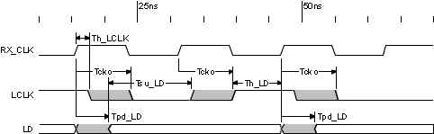
| Symbol |
Description |
Min |
Max |
Units |
| RX_CLK |
clock frequency |
|
64 |
MHz |
| divclk |
divided clock frequency |
|
32 |
MHz |
| Tpd_LD |
Data propagation delay time |
0 |
5 |
ns |
| Tcko |
Clock to output time for LCLK |
2 |
8.3 |
ns |
| Tsu |
LD setup time |
7 |
|
ns |
| Th |
LD hold time |
2 |
|
ns |
| Th_LCKL |
hold time for sampling LCLK |
2 |
|
ns |
Analyzed with timing designer gives a buffer at LD setup time of 5.6 ns,
and at hold time of 5.3 ns. The values of Tpdck and Tcko are taken from
MaxPlus timing analyzer. If major changes are done to the design these
calculations should be re-evaluated.
Bugs - Room for improvement
PCB
Loop-filter capacitors:
C27, C63, C13 and C95 should never be mounted according to final G-Link
specification.
Serial clock signal termination:
R9, R10, R22, R24, R25 should be 68 ohm instead of 22ohm to reduce
overshoot in clock signal.
Measurements clock signal quality should be made for further
optimizing this resistor value.
Motherboard need a dedicated clock signal for LSC. Better signal termination
on LSC UCLK could give better performance.
Swapped cables
In current version, LDC will come up even when cables arfe swapped, but
LSC will stay down. This is unfortunate since LDC Link Up led is more accesable
than the LSC Link Up led. One solution to this problem would be to specify
different reset signals for channel A and channel B. Thus neither channel
would see a reset if the cables are swapped.
LFF# and LDOWN#
User is only supposed to write data when LFF# is high, i.e. fifo not full.
When link is down LFF# should be high to assure taht no data is written
to LSC. Probably easy to implement by an AND-gate between LFF# and LDOWN#
internally in LSC FIFO.
Error recovery with different fiber lengths
In double channel version fibres must be of the same length within 1 meter.
If there is greater length difference, it is possible that the slave receiver
(B channel) data is delayed one clock cycle. The performance in this case
could be greatly improved by easy means. In the dbmux block of the LDC,
the state machine always look at channel A first for data. If channel B
data is delayed there will be data available the same clock edge, and then
should B channel data be chosen, and A-channel data should be registered
and sent next clock cycle.
Error reporting
Use of LD[3..2] in control words (signals error in channel A or channel
B) should be removed.
File to change: PARRX.VHD
Test mode
Flow control during test mode does not work when UCLK is <10MHz as LSC
FIFO gets stuck..
Sometimes in the double channel version, when leaving test mode, a control
word (UCTRL# low) 01000000 is written before link goes up. The error probably
lies in the FIFO logic assignments for dbldc. The error os no longer reproducable.
Return channel does not feature a test mode. Should be implemented.
Transmission frequency
One of the ideas of ODIN is to get the highest transmission rate and
still be running withing all the specs. XCLK could go up to 70MHz without
violating any specifications. This should be tried.
CERN - High
Speed Interconnect - S-LINK
Erik Brandin - 27 January
2000