
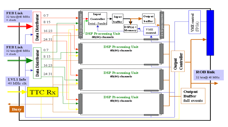
Table 1 Main characteristics of the ROD board in the baseline read-out architecture.
| Input links (32 bits @ 40 MHz) | 2 |
| Number of channels per board | 256 |
| Number of DSP Processing Units | 4 |
| Number of channels / DSP PU | 64 |
| Output links (800 Mb/s) | 1 |
| March 1999 | Connector types and pinouts being defined. End June schematics should be finished, prototype ready by fall 1999. |
| July 1999 | Design document ready (ATL-COM-LARG-99-011) |
| November 1999 | Transition module being defined |
| 27 March 2000 | Preliminary design review of transition module held at CERN. Ten transition modules will be built. ROD board under test. 40 "double G-LINK" receiver cards will be built. Will not use a P3 backplane yet, but a simple adapter. |
| 11 April 2000 | ROD board under test. Waiting for a transition module to be able to test more completely. DSP mezzanines needed adapter connectors to correct pinout |
| 27 June 2000 | ROD tested. S-LINK input and output tested. A new version of the PCB
will be made correcting some PCB design errors.
Vicente Gonzalez is trying to see if the LArg ROD can be used for the Tilecal as well. A problem may be that the incoming 32-bit data on the LArg ROD is handled in two 16-bit parts, while the Tilecal needs it to be handled on a complete 32-bit basis. |
| 2 February 2001 | With the S2VME64X transition module,
the LArg ROD has sucessfully sent data to a test program on a RIO.
Trigger rates upto 30 KHz could be handled with an event size of 1.2 KByte.
The test used the following S-LINK boards: SLIDAS (dummy data generation), S2VME64X transition module, ODIN (link) and for debugging a SLITEST, SLIDAD and SLIBOX have been used. |
| April 2001 | New ideas are taken up to design another version that has more input and output links on one board. In the July 2001 LArg week, the ROD Architecture Task Force with Bob Cleland as chair will decide what the final architecture will be, including the decision if the RODs will be upstairs or downstairs in USA15. |
CERN - High Speed Interconnect
- S-LINK
Erik van der Bij - 30 April
2001