Paper presented at IEEE Nuclear Science Symposium and Medical Imaging Conference 1991 in Santa Fe.
Published in IEEE Transactions on Nuclear Science Vol. 39 Num. 4 Aug 1992
A. van Praag *, T. Anguelov, D. Burckhart, R.A. McLaren, H.C. van der Bij, CERN, Geneva, Switzerland.
J. Bovier, P. Cristin, Creative Electronic Systems, Geneva, Switzerland.
M. Haben, P. Jovanovic, I. Kenyon, R. Staley, University of Birmingham, Birmingham, U.K.
D. Cunningham, G. Watson, Hewlett Packard Laboratories, Bristol, U.K.
B. Green, J. Strong, Royal Hollaway and Bedford New College, Egham, U.K.
Standard, fast, simple, inexpensive; is this not a contradiction in terms? The High-Performance Parallel Interface (HIPPI) is a new ANSI standard, using a minimal protocol and providing 100 Mbyte/sec transfers over distances up to 25 m. Equipment using this standard is offered by a growing number of computer manufacturers. A commercially available HIPPI chipset allows low cost implementations. In this article a brief technical introduction to the HIPPI will be given, followed by examples of planned applications in High Energy Physics experiments including the present developments involving CERN: a detector emulator, a risc processor based VME connection, a long distance fiber optics connection, and a HIPPI testbox.
High Energy Physics experiments have an impressive requirement for high bandwidth data transfers between scattered locations, to handle both the second-level trigger and event building. General purpose busses or links are not able to provide these high-speed transfers, and we assume that it should be possible to use synchronous unidirectional links to transfer the data from one point to another. We also assume that we will use a growing number of components supplied by industry; therefore it is important to choose a link that has the support of the major computer and peripheral Manufacturers.
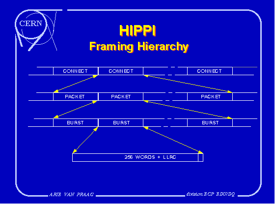
We have decided to use the High Performance Parallel Interface (HIPPI) to implement these links. The HIPPI specification was started in the Los Alamos laboratory in 1989 and is now an ANSI standard (HIPPI PH, X3.183-1991) [1,2]. This standard allows 100 Mbyte/sec synchronous data transfers between a "Source" and a "Destination". Seen from the lowest level upwards the HIPPI specification proposes a logical framing hierarchy where the smallest unit of data to be transferred, called a "burst" has a standard size of 256 words of 32 bit or optional 64 bit (Fig 1).However the size of a burst may be as small as 1 word only. Error checking adds 4 parity bits to each 32 bit word and one "LLRC" word that implements a lateral parity at the end of each burst. For each burst to be sent by the source, the destination needs to acknowledge in advance with a "ready" pulse. One or more bursts are combined in a "packet" without
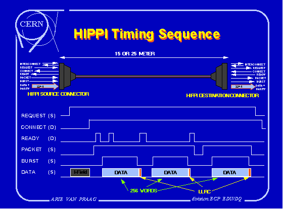
a given upper limit. To avoid partly empty bursts, one shorter than the prescribed size can be included in each packet. The same structure repeats for the "connect cycle" where the number of packets per cycle can be chosen freely. To establish a connection the source sends a "request" (Fig 2) to the destination which should acknowledge with a "connect" signal. Data put on the datalines during this request-connect handshake, which is called the "I Field", can be used to send information concerning data to be transferred, or can be used as a addressing information in the case a switch is used. Data transfer uses a 50 twisted pair cable of 15m or 25m. The clock is transferred through the cable with the data and has a rate of 25 Mhz which results in 100 Mbyte/sec synchronous data transfers. An optional second cable can double this throughput.
A silicon chip-set in the form of a source circuit and a destination circuit is commercially available from AMCC. These chips perform the hardware protocol encoding and decoding and interface at the HIPPI-PH level, including burst partitioning of the input data. The data inputs on the source and outputs on the destination are foreseen to interface with synchronous FIFOs. The ECL conversions for connection to the cable are done inside the chips. The destination chip uses a phased lock loop to resynchronize the clock, which is necessary for applications in switches. These chips have been successfully used in several applications.
HIPPI interfaces are commercially available from a growing number of computer manufacturers: the IBM 3090 and NEC mainframes, Sun and Silicon Graphics workstations. Network Systems Corporation has a VMEbus to HIPPI interface and makes a HIPPI crossbar switch. The latter has eight simplex channels or four full duplex channels and uses bits 0-23 of the I- field for routing. The least significant 4 bits are the actual output port address. By shifting around the address part of the I-field on each traversal of a switch, the final destination can reconstruct the path followed.
For the Large Hadron Collider (LHC) experiments the very high interaction rate and the enormous number of channels present severe problems in storing and moving data at all levels of the trigger and data acquisition chain. Several study projects for new detector and trigger logic have been approved by the Detector Research and Development Committee (DRDC).
The Detector emulator, known now as SLATE is designed to provide data at a rate, and a complexity, that allows realistic tests of the performance of links and processors chosen for use in second level triggers [3]. Flexibility is obtained by using software to create files of data describing the output of the detector. To make tests of different architectures as realistic as possible, physics generators and detector simulations are used to produce a data-base. A workstation is used to construct from this data-base, and from additional user data, the files containing the regions of interest. After formatting and adding the parameters for the physical output, these files are loaded into the emulator using ethernet. On receipt of a start signal the emulator loops sending partial event data. The use of hardware daughter boards provides the possibility to evaluate different physical outputs.
The emulator system is being built in VMEbus. Basically it is a memory whose size is defined as 48 bit by 64 Kwords. Information from simulations of the Spacal and TRD detectors indicate that areas of interest for second level triggers have a size of about 2 Kbyte. Using two units 500 events can be stored. To achieve the necessary transfer time of 10 msec/event, data must be transported at a rate of 100 Mbyte/sec. The first daughter board to be tested is a HIPPI source and uses the AMCC source chip [4].
VMEbus to HIPPI interfacing
The VMEbus to HIPPI interface is designed to allow the integration of HIPPI into VMEbus environments. VMEbus has been selected by the DRDC project RD13 [5] as a framework in which to prototype new hardware and software.
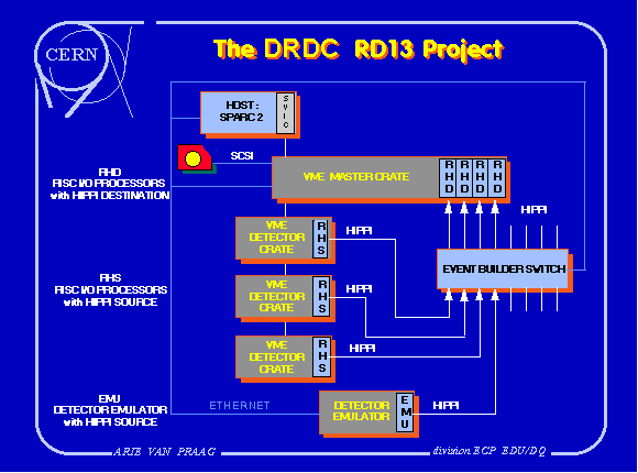
In RD13 (Fig 3) it is planned to use the commercially available HIPPI switch from NSC to build events. The idea of using a crossbar switch to build events is presented in a paper by E. Barsotti et al.[6]. In RD13 each detector crate will be equipped with an intelligent HIPPI source going to the crossbar switch to build the event in one of several destinations. The on board processors will analyze the data and good events are transmitted to the host computer.
For the HIPPI links the RIO 8260 processor board with a RISC R3051 microprocessor, equipped with a RIO HIPPI Source (RHS) daughter board, will be used. The RHS daughter board implements a HIPPI Source interface that is fully compliant with the HIPPI-PH standard. The processor sets up all data transfers and sends data from either the VMEbus or the local memory to the RHS. The RIO 8260 has a special mode to transfer data from the local memory to the RHS at a rate of 50 MByte/sec. The device has selectable modes to swap the bytes in the datawords, a feature needed if one sends data to computers with a different byte organization.
For debugging and testing purposes, the RHS has a step-by-step mode, is equipped with registers that can read back all data and control signals that are sent out, and can be tested under software control.
One of the first applications at CERN for HIPPI components will be in the L3 off-line area [7]. It is planned to attach several workstations via a HIPPI switch to an
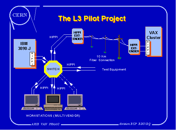
IBM 3090/200j system (Fig 4). This data analysis system is for the moment coupled to the on-line VAX 6300 data acquisition computer using a 10 Km fiber optic link runningat 1 Mbyte/sec. To cover this distance with increased speed we are developing the HIPPI Fiber Optic eXtension (HFOX) full duplex connection that replaces the standard 25 m copper cables.
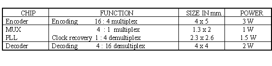
For serialization and deserialization of the 43 HIPPI signals the Hewlett-Packard chipset (table 1) is used [8]. This bipolar silicon chipset is specified for 16 bit parallel input at 75 Mhz and delivers with the encoding overhead a 1.5 Ghz serial output. The proprietary encoding algorithm achieves a good long term DC balance which simplifies stabilization of the laser-bias for constant output power. The interface to this chipset is a 1 to 3 multiplexer for the source coupling. The 25 Mhz HIPPI clock is used as input to the chipsets 75 Mhz phase locked loop. In the receiver the balanced code permits AC-coupling without signal degradation. The data is demultiplexed 3 to 1 to recombine the 43 bits and the extracted clock is divided down to the original 25 Mhz. HFOX is a collaboration project between CERN, Birmingham University and Hewlett Packard England.
All functions of the HIPPI source can run manually in single cycle mode, or under processor control with programmed cycle speed.
To allow CERN to test and maintain HIPPI equipment, a powerful test falcility is required. A tester has been developed at Los Alamos National Laboratories [9,10] and a second testbox is being constructed at CERN [11,12]. The CERN HIPPI testbox allows testing of HIPPI equipment both inside and outside the specifications. This includes the possibility of deliberately introducing errors. The main features of this testbox are:
Separate source and destination boards can be used individually to test HIPPI equipment, or may be connected together and the testbox can be placed in an existing link. Using the VME interface for processor control gives an extended range of possibilities and makes more accurate adjustments possible. Coupling the processor to Ethernet makes remote analysis possible. The remote control software will use TCP/IP. The user interface uses X-windows. The host machine will be a UNIX workstation. Analysis can be done from many types of workstations including the more sophisticated Pcs.
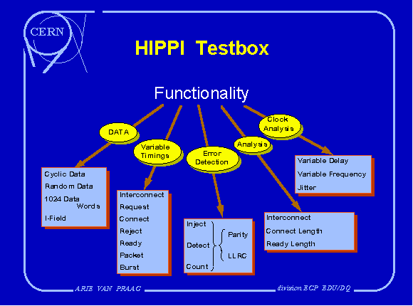
For source and destination the functionality can be divided in four subgroups, Data, Variable timings, Error detection and Analysis. The source (Table 2) cyclic and random data generator is a hardware implementation able to deliver data at the full
HIPPI speed. The 1024 x 40 Fifomemory is loaded with data via the VME port. The destination has the same size Fifo memory to store received data together with the Analysis bits. Variable timings on source, and destination (Table 3) are settings running from 0 to 15 or from 0 to 31 clock pulses for the indicated functions. Each has a default setting that corresponds to the minimum value in the specifications. The error detection part in the source can inject parity bits in every byte and LLRC errors on every bit and in any word chosen.The destination will store the error bits. Counters register up 256 errors for long term tests. The analysisgroup are functions used for remote analysis. However Clock Analysis has only manual controls and is used for clock stability and benchmark tests. The HIPPI testbox is being built using VXI crate and boards. To avoid timing constraints it is constructed almost entirely with ECL logic.
HIPPI is a new standard for fast point to point connections. It has a simple protocol which can be executed almost completely in hardware, keeping software overhead low. Interfaces are commercially available from several mainframe and workstation manufacturers. A commercially available crossbar switch can give network-like flexibility and can be useful in event building. A chipset is available as an industry product. The present distance limit of only 25 m can be extended by replacement of the cable with a serializer and deserializer interconnected with fast fiber optics to reach 10 km or more. VMEbus systems are being interfaced using HIPPI. Using these HIPPI components fast point to point connections can solve many of the data transport problems for data acquisition in the coming generation of high energy physics experiments.
The authors are very grateful to D. Jacobs for encouraging the initial work on HIPPI and to P.G. Innocenti, F. Bourgeois and Ph. Farthouat for the ongoing support. In addition the authors want to thank the people with whom we have discussed the use of HIPPI in data acquisition and especially R. Bock, L. Mapelli and R. Mount.
[1] High Performance Parallel Interface. Mechanical, Electrical and Signalling Specification (HIPPI- PH) X3.183-1991
[2] The High Performance Parallel Interface (HIPPI) and Ultra Speed Networks. Don Tolmie Los Alamos National Laboratory USA AIP Conference Proceedings 209 1990
[3] Embedded Architectures for Second-Level-Triggering in LHC Experiments (EAST), R.K. Bock & al. CERN/DRD/90-56 DRDC/P12, 30 October 1990
[4] HIPPI Source Daughter Board of the Detector Emulator ,T. Anguelov, CERN/EAST/note 91-12, 30 September 1991
[5] A scalable data taking system at a test beam for LHC, L. Mapelli*, P. LeDu, J. Harvey, E. Valente CERN/DRDC/90-46 P16 1990
[6] Effects of various event building techniques on data acquisition system architectures, E Barsotti, A. Booth, M. Bowden Fermilab, AIP Conference Proceedings 209, 1990
[7] Use of HIPPI/Fibre Channel to Build an Integrated Computing Environment R.P. Mount California Institute of Technology Pasadena, L3 Experiment CERN Geneva Switzerland, 30 November 1990
[8] A 1.5 Gb/s Link I nterface Chipset For Computer Data Transmission, R.C. Walker, T. Hornak, C.S. Yen, J. Doernberg, K. Springer Instruments and Photonetics Laboratory, HPL-90-105, July 1990
[9] High Speed Channel Tester, Purpose Summary and Status. Wally St. John, Los Alamos National Laboratory, C5; MS-B255 29 August 1989.
[10] High Performance Parallel Interface Tester Operating Instructions (user manual) Computing and Communications Division Networking Group (C5), Los Alamos National Laboratory 1990
[11] Testing and Benchmarking of HIPPI Interfaces, A. van Praag, CERN ECP/EDU/DQ/0191
[12] A Development System for the High Performance Parallel Interface (proposal), A. van Praag, CERN ECP/EDU/DQ/0390
28-Oct-91