.
![]()
This paper is presented by Arie van Praag as a breakout presentation in the PCI-week conference held from 27 to 31 March 1995 in Santa Clara, CA. The conference organizers have requested that the presentation covers both: possible future uses of PCI in HEP data acquisition and a detailed description of the PCI to HIPPI Interface under development for the NA48 experiment.
This report is published as CERN/ECP 95-4 3 January 1995
It is published in the PCI'95 Conference Proceedings March
1995 pg. 83-88.
Annabooks 11838 Bernardo Paza Court San Diego CA 921128-2414
A. van Praag, R.A. McLaren, J-P. Matheys, P. Vande
Vyvre, CERN, Geneva, Switzerland
T. Anguelov, G. Georgiev, S. Piperov, I. Vankov, INRNE - BAS,
Sofia, Bulgaria
D. Gillot, A. Guglielmi, Digital Equipment Corporation, Joint
project office, CERN
O. Orel, A. Sytin, IHEP, Prodvino, Russia
PART 1: Data Acquiosition for the LHC Atlas Detector
PART 2: Data Acquisition for NA48
Moving from Turbochannel to PCI
FIFO Memories and HIPPI Interfaces
Solving the Mechanical problems
Due to its very complex data acquisition systems High Energy Physics (HEP) experiments are always looking for cheap and fast computers and communication equipment. PCI as a mainstream product is one of the new technologies responding to these criteria. After a short introduction of CERN and its Particle Physics Facilities, the first part of this article describes, with a real development project as example, the specific problems of data acquisition systems in HEP experiments at the future LHC accelerator. Solutions where PCI technology will play a role will be presented, showing as examples the use of a VMEbus module with dual port ram and PCI to SCI interfaces. The second part describes the NA48 experiment including a detailed description of the development of the PCI to HIPPI interface.
In the war-ravaged Europe of the early 1950s, a far sighted group of scientists and politicians envisioned a new adventure in science, a European scientific laboratory. Even then, it was clear that state-of-the art science needed research facilities larger and more complex than individual nations could afford. In this way Europe's role in fundamental science would be restored, at the same time bringing together people from countries which had been at war only few years before. In 1954 twelve countries started to work on a 600 MeV Synchro-Cyclotron on the Meyrin Site in Switzerland. In Parallel CERN began to build the Proton Synchrotron (PS). This came into operation in 1959 and for a time was the most powerful particle accelerator in the world, supplying experiments with 28 GeV beams of protons. This accelerator is still in use as the first part of the actual system of interconnected accelerators.
In 1976 the PS was followed by a new more powerful Super Proton Synchrotron (SPS) machine of 450 GeV. This accelerator has a circumference of 7 Km and passes under the Swiss-French border.
In 1983 work started on the Large Electron Positron Accelerator (LEP). Constructed in a 27 Km tunnel, the first particles were accelerated during 1989, with an energy of up to 45 GeV. By 1995 LEP will reach an energy of 90 GeV.
On the 16th of December 1994 the CERN member states decided the construction of the Large Hadron Collider (LHC) in the same 27 Km tunnel, having two intersecting accelerator tubes with an energy of over 7 TeV each. During the short history of CERN the number of member-states has grown to nineteen. Four more countries have an observer status.
Several physics experiments will use the LHC accelerator. Three of them have already been approved: Atlas and CMS will study proton-proton collisions and ALICE will observe heavy ion interactions. An experiment consists of different specialized detectors each of them containing tens of thousands of channels. There are interactions in the detectors each 25 ns (40 MHz), but only a fraction of these is of interest. Filters are foreseen with several levels of triggers to select and store only selected data. In Atlas [4] the architecture uses three levels (LVL1, LVL2, LVL3) as shown in Fig. 1. At LVL1, special-purpose processors act on reduced granularity data from a subset of the detectors. The LVL2 detector trigger uses full granularity, full precision data from most of the detectors, but examines only regions of the detector identified
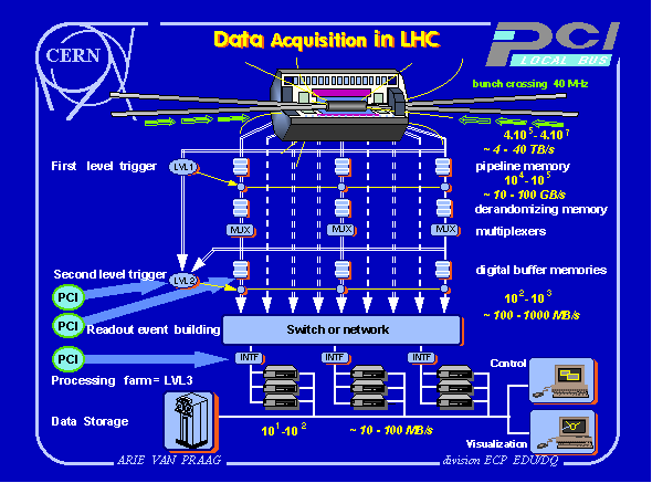
by LVL1 as containing interesting information, the so-called Regions Of Interest (ROI). At LVL3, the full event data is used to make the final selection of events to be recorded for off-line analysis. The LVL1 trigger accepts data at the full LHC bunch crossing frequency of 40 MHz (every 25 ns). The latency time necessary to form and distribute the LVL1 decision is ~2 s, and the number of positive decisions is expected to be 105/s. Hence the LVL1 trigger must select no more than one interaction in ~104. During the LVL1 trigger processing the data from all parts of the detector are held in pipeline memories. Requirements of the LVL1 trigger are that it must identify unambiguously the bunch crossing that contains the region of interest with a negligible deadtime. The LVL2 trigger must reduce the data rate from up to 100 KHz after LVL1 to ~1 KHz. Its architecture is based on the use of ROIs. The LVL2 trigger has therefore to access and process only small fractions of the data which reduces the required processing and data movement capacity. The processing is divided in two phases, extraction of the ROI and summarize it in a few data words, and combine it with information from other ROIs to make the LVL2 decision. The LVL2 latency is variable from ~1 to ~10 ms. After an event is accepted by the LVL2 trigger, the full data is sent, via the event builder, to the LVL3 processor farm where reconstruction of the physics phenomena is possible. Decision times are up to ~1 s. After the final selection made by LVL3, data will be stored at a rate of 10100 MB/s.
The planning for LHC is that it will be operational in 2004, and that the technology will be frozen in 1997. Standards will be used wherever possible. For the LVL1 part, the time available to do some very specific operations on the unfiltered data makes it necessary to construct the largest part of this front end with dedicated electronics.
Data accepted by the LVL1 trigger is transmitted to the digital buffer memories (Fig 1). Data input rates of 100 MB/s per memory are expected. Simultaneously, data from accepted LVL2 events must be output to the event builder. A dual port memory architecture with sophisticated memory management is therefore required. Currently
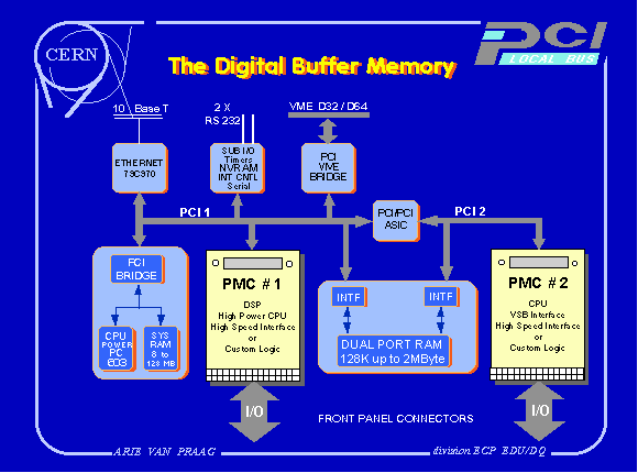
neither the input nor the output links have been chosen. Specifying the PCI bus as input and output to the digital memories, allows easier implementation of any link type. An example of a suitable module is currently being designed by Creative Electronic Systems (CES). The RIO2 VMEbus module [7] is shown in Fig 2. It has a Power-PC 603 or 604 as processor, 8 - 128 MB memory and a PCI main bus. One PCI Mezzanine Card (PMC) [2,3] slot is directly coupled to the main bus. The second PMC is coupled to this bus both via a PCI to PCI buffer, and via a dual port memory. The throughput of each memory port is 132 MB/s.
Referring again to Fig 1, the output of the digital buffer memories are transmitted through high speed links to the input of the event builder. The outputs of the event builder are connected to the LVL3 processor farm interfaces (INTF) This processor farm is built out of standard workstations. Most manufacturers have announced PCI on their new models. The link technology used can be (Serial) HIPPI or in the near future Fibre Channel Standard (FCS) or Scalable Coherent Interface (SCI). ATM is another possibility under evaluation. If we assume that the digital buffer memory and the LVL3 interface use PCI internally, then interfaces between the link technology and PCI are required. Possible solutions [10] for the system are:
1: HIPPI
The maximum throughput for HIPPI is 100 200 MB/s as given in the HIPPI-PH specification. Several HIPPI to PCI and Serial-HIPPI to PCI interfaces are under development by Genroco, Essential Communications and at CERN. No developments for the PMC form factor are known.
2: FCS
The maximum throughput for FCS is 100 MB/s as given in the FC-PH specification [6]. Several PCI to Fibre Channel and PMC to Fibre channel interfaces are under development in industry by among others Western Digital, Emulex and Interphase. One of the difficulties is to combine the standard optical FCS modules with limited dimensions, especially height, of the PMC.
3: ATM
ATM specifies speeds from 155 Mb/s up to 2.4 Gb/s, where 1.2 Gb/s corresponds with 100 MB/s. PCI to ATM interfaces are under development by several companies, for example Newbridge, Efficient Networks and Digiboard. The development of an ATM PMC is under evaluation as part of a collaboration between at CERN and Uppsala University. All these interfaces cover the 155 Mb/s speed only.
4: SCI
The maximum link speed in the SCI specification is 1 GB/s. A development project for a PCI to SCI interface has been started at CERN. The interface to the PCI bus will use the AT&T Orca FPGA, for data and PCI bus control, as shown in Fig 3.
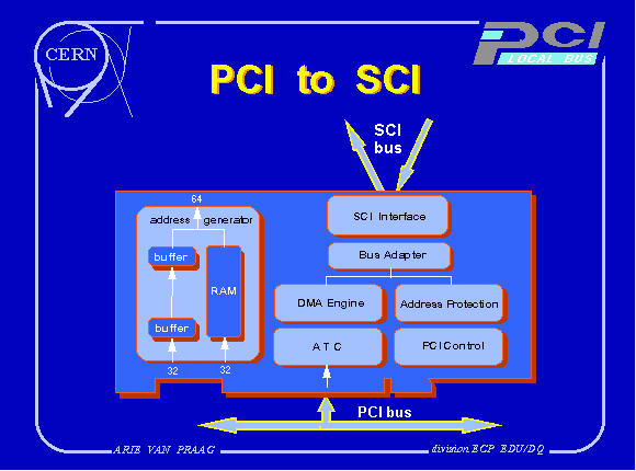
The internal logic of the card is built with a DMA engine and address protection logic both implemented in PALs. They couple via a bus adapter to the Cbus entry of the SCI interface, a Dolphin Nodechip. The 64 bit SCI address is built by storing a number of the high words (A32-A63) in RAM and passing the low word (A00-A31), via the necessary buffers for bus adaptation, directly from the PCI bus to the SCI interface.
A very similar PCI-SCI interface but including a 256 word bi-directional FIFO in the data path is being developed by Manchester University in collaboration with CERN [8]. It is intended to be used in the Atlas LVL2 trigger.
The NA 48 is a CP violation experiment. It is now in the construction phase. It should be fully operational in 1996 and finish before the installation of LHC.
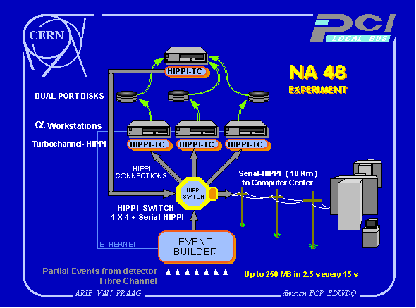
In the NA 48 experiment a few thousand events per second are expected after the second level trigger (LVL2) during every accelerator cycle (a spill of ~2.5 s every 15 s), resulting in a data block of up to 250 MB [9]. These data are then to be processed by the third level trigger (LVL3) which requires the power and flexibility of powerful workstations. Three sequential interleaving workstations are used because processing of this quantity of data needs more time than is available between two spills. The very high event rate does not allow any software intervention during the data transfer. Local disks are used for storage, complemented with a 10 Km high speed fiber optic link to the central computer center. Fig 4 shows an overview of the system.
Spill distribution is based on point-to-point HIPPI connections. The data block is distributed spill by spill using a HIPPI crossbar switch. The processors are DEC Alpha workstations with TURBOchannel interfaces. As part of a joint project, HIPPI to TURBOchannel interfaces were developed at CERN [5]; the OSF/1 device drivers were developed by DEC. On top of the driver is a user level library. Tests with this architecture have shown that 64 MB of data can be transferred in ~770 ms from the event builder to a DECstation AXP 5000/200, including software overhead and Ethernet feedback to the data source. This corresponds to a transfer speed of 83.1 MB/s. Block sizes larger than 64 MB could not be tested because of the limits in the OSF/1 version 2 operating system. The very recent OSF/1 version 3 does not have this limit and tests with block sizes of up to 250 MB have been performed. To connect to the central computer center, one port of the switch is equipped with a Serial HIPPI module. The connection is made with single mode fiber optic cable.
In the future more powerful workstations are needed. DEC has announced that new workstations will no longer support TURBO channel, instead they will be equipped with PCI interfaces.
In a new joint project the former partners have therefore agreed to develop a PCI to HIPPI interface that meets the NA48 specifications, adapting at the same time the drivers but maintaining the user level library. In parallel new industrial PCI to HIPPI and PCI to Serial-HIPPI interfaces will be evaluated as they become available.
The HIPPI to PCI modules are built around a PCI interface with a DMA Engine, a Scatter Gather Memory, a History Memory, and the HIPPI Interfaces. The block diagram for the Destination is shown in Fig 5. The only differences for the Source are that the data flow goes in the opposite direction and the use of a different HIPPI circuit.
As CERN developments are often very specialized, quantities for economic use of ASICs are rarely reached. For this reason the PCI
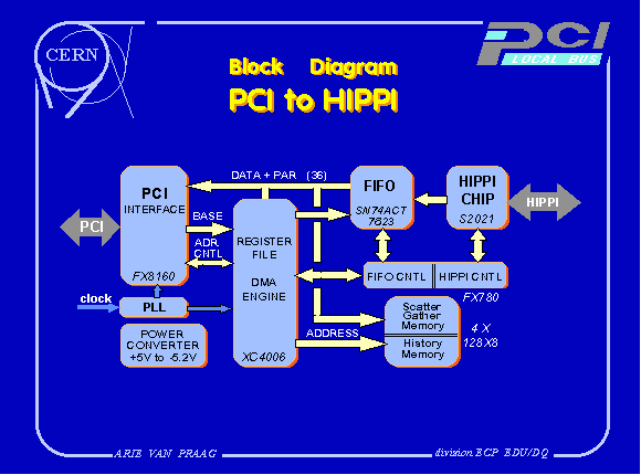
interface has to be implemented using programmable logic. The only FPGA for the PCI interface, available at the start of the project, that is fully compliant with the PCI AC-drive parameters was the iFX8160. This FPGA is complemented by a Xilinx XP 4006 containing register files, the DMA engine, and the memory control. As the iFX8160 has no possibilities to bring a buffered clock to the output pins an external Phased Lock Loop is used for clock distribution.
All interrupts except "End of Transfer" will be masked during transfer. To allow a simpler way of event building by using the connectivity control of the switch, an external interrupt on the back panel will be included and can replace the "End of Transfer" with an external signal coming from the system, such as "End of Spill".
In order to allow the sustained speed for receiving very large blocks of data, the host processor should not interact in the transfer process. In the HIPPI destination and in the HIPPI source, this is done by including a Scatter/Gather Memory and a History Memory. For every page boundary a scatter/gather index addresses the scatter gather memory and a new address is loaded into the DMA write pointer. This is the first address of the new page to be accessed. From here the DMA write pointer increments for every word transferred. At the end of the page a new page address is fetched the same way from the scatter/gather memory. The size of the scatter/gather memory is system determined, and depends on the number of pages required to store the maximum allowed quantity of data. At present 64 KB is foreseen which corresponds to a 256 MB transfer block on an Alpha DS 5000/200, and 512 MB on the new PCI stations. Bit 31 indicates the last page allowed for the current transfer. The scatter/gather memory must be initialized by the processor before start of the transfer, using I/O operations.
For the same reasons of speed, the pointers and messages concerning the transfer are not forwarded to the host, but stored in a history memory. Tags contain such data as "Burst Status", "End of Packet", "End of Connection" and LLRC and Parity errors. The offset to the beginning of the transfer is stored with the tag. The processor can access the history memory only after the transfer is finished, using normal I/O operations.
Scatter/gather memory and history memory fit together in a fast 4 MB (4 x 128x8) static memory that is included in the normal PCI address space of the Source and Destination boards as follows:
   Base Address  Address Window       Unit           XXX         00000-3FFFF      Registers
      XXX         40000-7FFFF        FIFO
      XXX         80000-BFFFF    Scatter/Gather
      XXX         C0000-FFFFF    History Memory
FIFO Memories and HIPPI Interfaces
Due to the 10 Km link to drive, large FIFOs, in the order of 4 Kwords (2 X 74ACT3651) are necessary. The HIPPI interfaces are built around AMCC circuits, the S2020 for the source and the S2021 for the Destination. A power converter generates the necessary voltages for HIPPI.
Mounting two 100-pin HIPPI connectors for a full
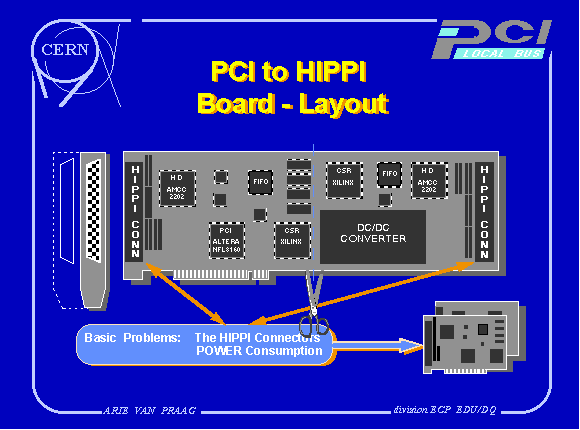
duplex interface needs a double-width back panel, or a special solution. Using an I/O cable into a remote connection box is too delicate in a HEP experiment environment. The logical solution is two independent units, one as a HIPPI Source and the other as a HIPPI Destination, as shown in Fig 6. At the same time the power dissipation per module is within the limits of the PCI specifications.
Looking in depth at the present Alpha station, its internal circuitry uses the 21072-AA IC. An interesting point is that this processor bus to PCI interface chip, according to the datasheet, shows asymmetrical throughput for different speeds and modes:
Mode     Read/Write Speed MB/s  HIPPI Function   DMA         W          120      Destination
 DMA         R           70        Source
Pr.I/o       W           84      Destination
Pr.I/O       R           22        Source
To obtain speeds in the 70 - 80 MB/s range, the best results can be obtained if the HIPPI Destination uses DMA mode. However, programmed I/O seems to be fast enough. The HIPPI Source will have much better throughput using DMA transfer. During DMA transfers the processor should be idle; if programmed I/O is used the processor should only do the transfer and no other tasks.
A prototype board has been mounted and is ready for tests. The rather simple implementation needs wait-states during set-up and page switching. This means that speeds will probably not be better than 60-70 MB/s, and as such not fast enough for the final needs of NA48. Having this solution working, the project will be continued with the development of 64-bit PCI interfaces where the 100 MB/s speed of HIPPI can be sustained. In this second version both Source and Destination modules will have both programmed I/O and DMA transfer possibilities.
Data acquisition for HEP has always been looking for more computing power with faster interconnect possibilities. In the past this was done with dedicated electronics and interfaces. The PCI gives the physics community an I/O bus standard that is fast enough to solve a many of its speed problems. In addition, HEP experiments have a lifetime from design to end of operation of 20 years. This spans several generations of computer technology, therefore the interconnections have to be as flexible as possible. PCI and PMC offer a fast, processor independent, industrially supported solution.
PCI could be used on many places in future HEP data acquisition systems and its influence will certainly go much further than the few examples described here.
![]()
This is one of the CERN High Speed Interconnect pages - 17 July 1995 - Arie van Praag