

S-LINK News 1999
TileCal plans to use G-LINK based S-LINK at front-end link
15 December 1999. Jim Pilcher and his collegues of the University
of Chicago who are responsible for the front-end links of the TileCal,
have made radiation tests on the Simplex G-LINK
card that is based on the 'old' G-LINK HDMP-1022 and Actel components.
Their article "Neutron
Irradiation Tests of an S-LINK-over-G-link System" has the following
conclusions:
The survivability of the S-LINK-over-G-link system under neutron irradiation
has been satisfactorily demonstrated. The system continued to operate at
10 times the required neutron fluence.
The observed rate of single-word errors would correspond to 6.7 per
month from the entire ATLAS TileCal system for the nominal neutron fluence.
Since these errors are detectable from parity information, and since the
data itself has considerable redundancy, this error rate should not pose
a problem; nevertheless, the ROD modules which receive the data must test
for these errors and take appropriate action. The actual error rate in
ATLAS should be lower because the link will only be used with a duty factor
of ~50% of that used here.
The observed rate of block errors would correspond to 0.53 per month
from the entire TileCal system. Such errors would result in the loss of
all data from one electronics drawer (1/256th of the system) for a number
of consecutive events. If these errors correspond to loss of link synchronization
the recovery time is estimated to be ~ 0.5 ms. At the maximum LVL1 trigger
rate this would correspond to a block of ~ 40 events. The fraction of LVL1
triggers affected by such an error would be ~10-10. Such a loss
appears entirely acceptable but an ATLAS-wide policy would be helpful for
reaching a conclusion. These block errors correspond to a bit error rate
on a single link in the nominal TileCal neutron environment of 4x10-13.
During this test the LSC was exposed to 9.9 Krad of ionizing radiation.
Separate studies have indicated that the system remains fully functional
to over 20 Krad.
The S-LINK team encourages this type of radiation tests as they cannot
guarantee that the links they build are tolerant to radiation. This remains
the responsability of the physicists who are building the final system.
The Simplex G-LINK card was a best-effort
to design a radiation tolerant link, and even that one has shown that there
were problems with certain components and bit error rates. Note that the
Simplex G-link cards can be made commercially available if there is sufficient
demand. For the testbeams where there is much less radiation, the TileCal
is currently using the FCS-LINK,
which is commercially available.
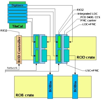 |
TileCal testbeam Read-Out Crate based on commercial components
15 December 1999. The Read-Out
Crate of the ATLAS Tile Calorimeter that is being designed for the
testbeams in the year 2000, will be completely based on commercially available
components.
One RIO2 processor from CES will be able to handle three front-end links
that come from the detector and one read-out link that goes to the Read-Out
Buffer.
Both the front-end links and the read-out links are S-LINK based. The
front-end links used in the testbeams are the commercial available FCS-LINK,
which have been used already since the 1999
testbeam. Those links will not withstand the radiation levels that
exist in the final ATLAS system. |
ODIN: a new optical link running at 128 or 160 MByte/sec
13 December 1999. Based on the new low-power G-LINK chip from Hewlett
Packard a new S-LINK has been built. As the
link is fully compatible to the S-LINK specification, it can be used as
a drop-in replacement of any of the other links such as the ones based
on Fibre Channel or SCSI/LVDS components. The newly developed link is able
to sustain a data rate of 128 MByte/sec, or, when two fibres are used in
the forward channel, it can even sustain a rate of slightly less than 160
MByte/sec.
All of the components on the new card are powered by 3.3 Volt. As currently
most motherboards power the link cards with 5 Volt, a drop-down regulator
can be put on the board. When ordering, one should mention the required
supply voltage. The supply current is typically 1.0 Amp for the single
G-LINK version. This is only 3.3 Watt when the card is supplied with 3.3
V, or 5 Watt when supplied by 5 Volt. The numbers are about 20% higher
for the double G-LINK version. Other features are that the link uses the
new Small-Form-Factor (SFF) optical transceivers from Infineon, which use
the new VF-45 fibre-optic connector,
also called Volition. The advantage of this connector is the low-price
for both the optical cable and the transceiver as it works with connectors
without a ferrule. This helped considerably in getting the component price
down by 25% compared to that of the FCS-LINK2 card in 1998 (while even
improving the performance by 25%).
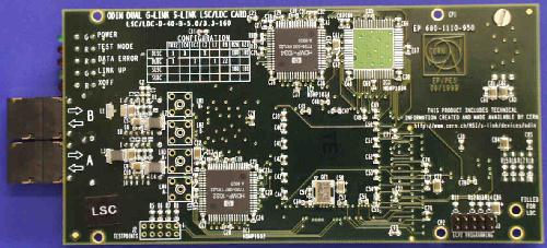
Erik Brandin, a Swedish student from KTH, nicknamed the link ODIN,
which stands for Optical Dual g-lINk. The other developers were Zoltan
Meggyesi, who also designed part of the Fibre Channel S-LINKs, Erik van
der Bij who designed the PCB and Robert McLaren who guided the project
so it could be finished in time before both Erik Brandin and Zoltan Meggyesi
left CERN.
The ODIN will be commercialised by the Hungarian company CERNTECH.
Zoltan Meggyesi is also active in CERNTECH, which means that CERNTECH can
update the PROM of the link when necessary. The Fibre Channel link is also
still available from CERNTECH and is the fibre-optic link of choice until
the first production run of ODIN cards is available in May 2000. Until
then, a few of the prototypes built at CERN will be available to selected
experiments.
All features of the link can be found in the ODIN
Datasheet (.pdf).
1 nA/bps
30 September 1999. A typical S-LINK such as the Fibre
Channel link, draws only 1 Amp from the 5 Volt power supply when it
transfers data at one gigabit per second. This is only one nanoamp per
bit per second. This 5 Watt is less than the maximum of 7.5 Watt that the
S-LINK specification allows. Newer links likely will consume even less
as mainly 3.3 Volt components will be used.
Main features revisited
29 September 1999. After four
years of existence, the S-LINK specification
is well known. But as the specification has been stable for over two and
a half years, for many designers it has been quite a long time that they
read the complete specification. Therefore it may happen that some of the
features are forgotten or not completely understood when an S-LINK motherboard
is being designed. Four of those features will be revisited here: control
words, error detection, flow control and reset.
All S-LINKs have a way of sending control words, as opposed to
sending normal data words. Those words can be used for encapsulating the
data to transmit in between "start of fragment" and "end of fragment" control
words, like used in the ATLAS experiment. In this case the "end of fragment"
control word will also contain the transmission error information of the
fragment's data and the control word itself. Like normal data words, control
words can contain any data, except that only 28 bits can be used (see the
table below). Two of the lower four bits are used for error detection information
and another two are reserved for future use. It is very advisable to
use control words as if you don't, your data will be transmitted as
a single stream without you knowing where the begin and end of each data
block is. Also it would be impossible to get error detection information,
as that is only sent out together with control words (except for links
that have an word-by-word error detection mechanism like parity).
All S-LINK links have a mechanism (using either CRC or parity) that
can detect errors that are introduced during the transmission of
data. If an error is detected, the S-LINK destination card (LDC) will set
a bit in the control word that ends the block of data sent (see
the table below). So the S-LINK inserts the error detection information
inside the stream of data. Therefore it is advisable to also store the
control words in the memory.
Data line meanings when LCTRL# is low
| LD[31..4] |
LD[3] |
LD[2] |
LD[1] |
LD[0] |
| Same as UD[31..4] |
Reserved for future use |
Reserved for future use |
When 1: Transmission error in Control Word.
When 0: Control Word OK |
When 1: Transmission error in previous data block
When 0: Previous Data Block OK |
All duplex S-LINKs have a simple mechanism for flow control, i.e.
with the UXOFF# signal the read-out motherboard can tell that it is "almost
full". The LDC will transmit this to the LSC where the Link Full Flag LFF#
will tell the front-end motherboard that it should stop sending data immediately.
In fact it may still send two words after LFF# became active. The LFF#
signal not only gets asserted when the receiving side is almost full, but
also when the front-end motherboard sends data faster than the physical
link can handle. E.g. on a Fibre Channel S-LINK card, the words are transmitted
at a speed of 27 MHz, while the S-LINK LCLK can be up to 40 MHz. To throttle
the speed, the LSC will make LFF# active for on average one third of the
time (1 - 27/40). This still gets you up to a considerable speed of 103
MByte/sec.
Also simplex links have the LFF# signal as also there the S-LINK clock
which may be up to 40 MHz, may be faster than the physical link can handle.
Therefore
all front-end motherboards should be able to handle the LFF# signal as
otherwise data will get lost.
An S-LINK needs a reset to start working. On the links that have
been built up to now, both the LSC and LDC need an independent reset. Duplex
links that will be built in the future, such as the ODIN,
will allow you to reset only one side, after which that side will also
reset the remote side. Note that there is an handshake protocol between
URESET# and the LDOWN# signal which should be respected. Having URESET#
in a writeable register and LDOWN# in a readable register and some software
will do the job.
NA48 has taken this year 170 TeraByte of data over S-LINK interfaces
6 September 1999. Last year the NA48 experiment has made an major
upgrade of the data acquisition system
in which every bit of the physics data goes through one of eleven S-LINK
to PCI interfaces, which are controlled by a Linux
driver. Last year the interfaces had moved 75 TeraByte of data, while
during this year's run they moved another 170 TeraByte. None of the eleven
interfaces has shown any failure during those two years.
S-LINK in CERN's Technology Database
 27
July 1999. S-LINK is one of the technologies that comes from CERN that
has applications outside the High-energy Physics community. It has already
been used for moving display data (Olivetti and Oracle research labs) and
in telescopes (Megacam), while people have shown interest in using it in
areas such as in the offshore industry (underwater towed vehicle) and for
moving data out of a digital camera.
27
July 1999. S-LINK is one of the technologies that comes from CERN that
has applications outside the High-energy Physics community. It has already
been used for moving display data (Olivetti and Oracle research labs) and
in telescopes (Megacam), while people have shown interest in using it in
areas such as in the offshore industry (underwater towed vehicle) and for
moving data out of a digital camera.
Of course there are many other developments at CERN that may be of interest
to others. The CERN Technology Database
contains information on technology developed and in use at CERN. It is
compiled and maintained by the CERN Industry and Technology Liaison Office
(ITLO) in collaboration with the relevant CERN Divisions and Groups. It
aims to make available information on such technology to industry in CERN's
member states, "as is" or via a licence agreement, and to disseminate such
information within CERN and its collaborating institutes.
The database also serves as a point of contact for the flow of technology
information to and from CERN. It is used to gather information on CERN
technology directly from sources within CERN as well as to channel enquiries
on CERN's technology from Member States, collaborating institutes and from
CERN itself to the appropriate sources of information. These enquiries
will include requests for details of technologies as well as information
on consultation services.
To have an idea on how the information is presented, have a look at
the S-LINK
entry of the CERN Technology Database.
 COMPASS
received 20 Fibre Channel S-LINK cards from Hungarian company
COMPASS
received 20 Fibre Channel S-LINK cards from Hungarian company
9 July 1999. On 22 June Cerntech,
the Hungarian company who produces the
FCS-LINK, shipped 20 FCS-LINK cards (10 LSC, 10 LDC) to COMPASS. Together
with the cards COMPASS has already, they will make up for the 12 links
that COMPASS needs for testbeams to be held in the second half of 1999.
The data will be received by 12 spill
buffer cards (S-LINK to PCI cards with a large FIFO-like organised
memory on the S-LINK side) for this purpose as well. The design of the
final read-out
driver, called CATCH, is also well under way.
Gazing in space with SHARCs, S-LINK and VxWorks
9 July 1999. Jean de Kat and his collegues from CEA-Saclay, Dapnia/Sei
have written a VxWorks driver for the S-LINK to PMC card. The software
has been tested on a Motorola 2604-333MHz-64MB VME processor board. With
the SLIDAS as a full-speed data generator, a transfer rate from S-LINK
into the Motorola's memory of 82 MByte/sec has been measured. This is largely
enough for his MEGACAM telescope application
in which the CCD camera data is coming from a SHARC link (max 40 MB/s)
before it is transferred over an FCS-LINK to the Motorola processors.
April-June: too much progress
9 July 1999. In between April and June many things have happened,
which made there was little time left for updating the pages.
S-LINK pages split
19 March 1999. Like with stock values, when the value gets too high,
they do a stock-split. This time the S-LINK web pages became too long to
be easy to use and therefore the S-LINK Products
and Projects pages got each their own page.
Also the area "people using S-LINK" got
removed as the list was becoming too long to maintain.
G-LINK Link Source Card ready, installation in test beam
19 March 1999. The G-LINK Link Source
Card that uses the Hewlett Packard HDMP-1022 serialiser is working.
The board, which uses an Actel A54SX16 FPGA as protocol chip worked first
time. This was a great accomplishement (and a fortunate one) as the Actel
is a one time programmable device. Zoltan Meggyesi implemented a data generator
in the Actel. In fact three different generators are implemented, each
one designed in a different way so the influence of the design method (e.g.
triple redundancy) on the radiation tolerance can be tested. At the end
of March the card will be installed next to the SPS in building 889 to
do the radiation tests. The corresponding G-LINK
Link Destination Card was working already before and has been used
on 11 March at the Paul Scherrer Institute to test the sensitivity to upset
of the serialiser chip that Peter Denes designed.
COMPASS CATCHes on
9 February 1999. For the COMPASS experiment a readout-driver and
buffer-module called CATCH
(COMPASS Accumulate, Transfer & Cache Hardware) is in development.
The FPGA based VME module serves as an interface between the front-end
of the detector systems and an on optical S-LINK, which transmits the data
to the Readout
Buffer (ROB). It also acts as an fan-out for the COMPASS trigger distribution
and time synchronisation system (TCS). The readout-driver monitors the
trigger and data flow to and from the front-ends. In addition a specific
data buffer structure and sophisticated data flow control is used to pursue
local pre-event building.
LHCb will use S-LINK in the prototype Readout Unit
2 February 1999. The LHCb experiment will use S-LINK
in the prototype of the Readout Unit. The Readout Units (RU) receive
event fragments from several frontend links and assemble them into
larger subevents. Once a subevent is assembled, the RU transfers it
to the next stage for further event building. In the final system 100 Readout
Units are needed. Each unit will receive between one and four S-LINK inputs
(LDCs) and may have one S-LINK output (LSC). The design of the RU has been
started and it expected to have a first working prototype ready in Summer
1999.
With this decision, LHCb is the fourth high energy physics experiment
(after NA48, ATLAS and COMPASS) where all of the physics data taken may
be sent over S-LINK.
 S-LINK
Studies in the TileCal ROD Environment
S-LINK
Studies in the TileCal ROD Environment
2 February 1999. Two
S-LINK cards have been tested at Valencia ROD Lab using different S-LINK
hardware devices and hosts. In the source side a PC PentiumII 266Mhz running
Linux kernel 2.0.35 allocate a PCI to Slink board. At Receiver side a Motorola
2604 VME card under LynxOS 3.0 allocate a S-LINK to PMC card. The main
goal of the test was to try to parametrize in terms of Bandwidth the current
commercial S-LINK hardware devices. One of the conclusions is that CTRL
DMA Transfers (DMA buffering with CTRL words) the transfer rate can reach
up to 85 Mbytes/sec for 8Kwords (the maximun Packet size provided by the
SLIDAS data generator). In terms of Bandwidth, the penalty coming from
the software CTRL words switch, which is nicely seen in the curves, it's
about 10% for 1Kword. Without control words, a speed of 89 MByte/sec can
be measured.
Q: Can S-LINK logic easily be integrated onto a motherboard?
A: Yes!
1 February 1999. Currently all S-LINK links are implemented as daughter
cards of the size of a PMC card. To reduce cost, it is foreseen that in
final applications the link logic may be integrated on the front-end motherboard
or on the read-out motherboard. As currently most designs are prototypes
and as link technologies are still rapidly changing and are becoming cheaper,
it is still too early to integrate the link logic on the motherboards.
However, we have to learn already now if any difficulties will arise
if S-LINK logic is integrated with other logic. One may think of problems
of the co-existence of gigabit signals on boards with other frequencies,
EMC, noise on power supplies etc. To get experience with this, Wieslaw
Iwanski of the Institute of Nuclear Physics in Krakow has integrated the
Fibre
Channel Link Destination Card logic with S-LINK
to PMC card logic. In the last week of January he has tested a prototype
in both a VME environment and inside a PC (with a PCI to PMC adapter).
The board has been working without any problems during more than a day
while it received full speed data with different patterns.
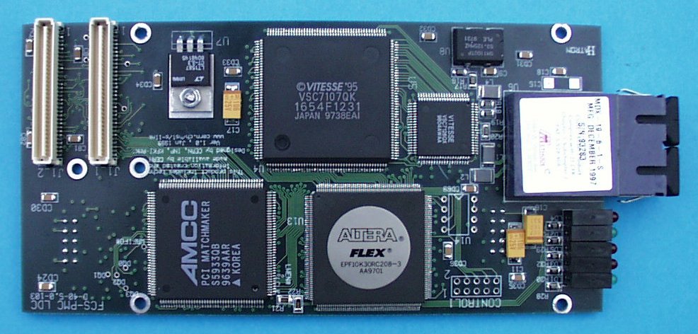
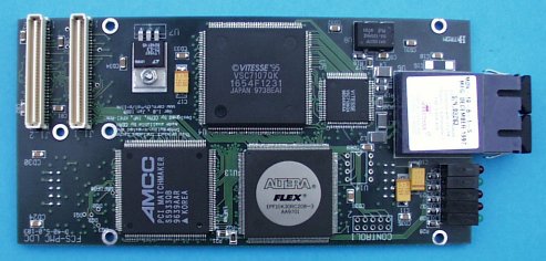 |
FCS-LINK LDC and S-LINK to PMC card integrated |
As the board has the gigabit signals differently routed than the original
FCS-LINK2 it shows that when integrating it is possible to redo the layout.
Of course one has to keep in mind the high-speed design techniques such
as putting decoupling capacitors as close as possible to the pads of the
chips and optical transceiver, having a controlled impedance for the differential
lines carrying the gigabit signals etc. Therefore it is recommended to
have someone from the S-LINK team review your design before doing the final
layout.
Wieslaw will send three of those boards to CERN, where they will be
tested over a long period. After that, they may be used in testbeams or
in the DAQ Prototype-1 project.
In those projects the new board will be more practical as it is only one
slot high, while with the solution used until now, two VME slots were needed.
Until now it is not foreseen to have this board commercially available.
Soon a web page will be made describing the integrated FCS-LINK2 and the
S-LINK to PMC card.
Simplex G-LINK LDC robust
25 January 1999. In the ATLAS experiment there are some detectors
that would like to use the S-LINK protocol on the front-end
links. That means that they like to use the signal description and
the protocol. In the area where those links are going to be used there
is a certain level of radio-active radiation, which needs special radiation
tolerant IC's that can withstand this. This area is full of unknowns, so
there are several projects working on aspects of the radiation tolerant
IC's and logic.
Zoltan Meggyesi is researching if
normal, commercial, programmable chips are radiation tolerant enough,
and is also looking at the different design techniques that can be used
so that the logic can withstand single bit errors.
Another problem area is the serialiser IC's that need to be radiation
tolerant as well. Currently there is no chip available that is known to
withstand the radiation levels that ATLAS needs it for. Preliminary tests
have been made with the G-LINK serialiser from Hewlett Packard, but during
radiation the receiving G-LINK lost its synchronisation too often and also
the error output was too often active. Note that in those tests the data
itself has not been tested for errors. But it might still be that the G-LINK
is suitable as the radiation levels used during the tests were much higher
than those during the running of the LHC. Therefore extra tests will be
performed. Also, in the CMS experiment, a serialiser chip is being designed
which sends data in a format so that it can be received by a G-LINK receiver.
To help those different projects in testing chips for radiation hardness,
the G-LINK Link Destination Card has been
built. Prototypes have been tested and are very robust. Because of special
power decoupling and EMC techniques the board even works with a supply
down to 4 Volt and even at high temperatures (without a cooling tower),
the board receives data without failure. As an engineer from a company
that uses G-LINK chips in commercial designs stated: "That is absolutely
amazing! I definitely think I'll try your localized ground plane on the
next design we do with G-LINKs. I would love to be able to leave those
cooling towers off of the G-LINKs".
We have designed a G-LINK Link Source card as well, which will be used
in Zoltan's radiation testing project. Prototypes are expected by the middle
of February.
NIKHEF makes CRUSH
8 January 1999. The Compact Robin
Using the SHarc (CRUSH) is a design of an ATLAS Read-out buffer.
The board receives it's data over an S-LINK connector, stores in a 1 MByte
Zero Bus Turnaround RAM and can process it with the SHARC processor. All
communication with the board is done over the six SHARC links. Although
the board is in the PCI form factor, the connector is only used to draw
power from it.
Old S-LINK News
CERN - High Speed Interconnect
- S-LINK
Erik van der Bij - 2 May 2000