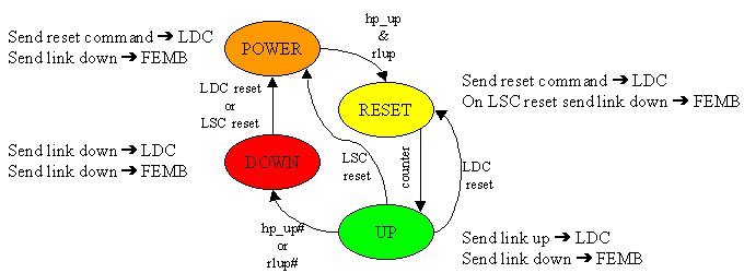
Figure 1. LSC Power-up and Reset State Machine
Erik van der Bij
( CERN-Geneva)
1. Forward Channel
1.1 Normal Frames
1.1.1 Data Frame
1.1.2 Control Frame
1.1.3 HOLA Link Command
1.1.4 Transmission example
1.2 Test Frames
1.2.1 Test Control Frame
1.2.2 Test Data Frame
2. Return Channel
3. Test Function
4. Reset Protocol
5. Architecture of the Link Cards
5.1 Transceiver
5.2 Link Source
Card
5.3 Link Destination
Card
6. Power consumption estimation.
The HOLA S-LINK interface is a standard S-LINK implementation which
uses the TI TLK2501 2.5 Gbps transceiver both for the forward and for the
return channel (one per card). For the optical transmission Small
Form Factor Pluggable (SFP) Multimode transceivers with LC Connector
are used. As opposed to the ODIN S-LINK, the HOLA can transfer with one
duplex fibre at the full S-LINK bandwidth of 250MB/s. To achieve this rate,
the input UCLK clock can be increased up to a frequency of 62.5 MHz. Output
clock in the LDC (independently of UCLK frequency) can be also chosen to
be 62.5 MHz (40 MHz default value).
The design is not intented to be used in an environment with radiation.
IDLEs consist either of the sequence <K28.5,D5.6> or <K28.5,D16.2>.
Control words are distinguished from data words by a preceding special HOLA Command (Next word Control Word (NCW) - for further details see 1.1.2).
The most significant bits, D[31..16], are sent first, followed by the least significant bits, D[15..0], on the next clock cycle.
4kbyte (1024 data words) is the maximum Payload size of a data frame (for bigger payloads the error detection capability of the CRC would degrade). The transmission of a data frame will start when a data word is transferred from the FEMB to the LSC input buffer. The frame will be closed with CRC generation in the following cases:
Even parity is used as error detection for control words. Even parity
is chosen so that a control word containing all zeros will have all parity
bits also zero. The 4 least significant bits of the word are used for this
purpose, as shown in the table below:
|
|
|
|
|
|
| Control Word | Even parity bit for D[31..25] | Even parity bit for D[24..18] | Even parity bit for D[17..11] | Even parity bit for D[10..4] |
All of them begin with 2 consecutive K23.7 characters, followed by the
corresponding code, as described in the table below:
|
|
|
|
| K23.7 K23.7
0000000000000000 |
|
Remote reset off |
| K23.7 K23.7 0000000000000001 |
|
Remote reset |
| K23.7 K23.7 0000000000000010 |
|
Next word a CRCC |
| K23.7 K23.7 0000000000000011 |
|
Next word a control word |
| K23.7 K23.7 0000000000000100 |
|
Test mode off |
| K23.7 K23.7 0000000000000101 |
|
Test mode on |
| K23.7 K23.7 0000000000000110 |
|
Link Down |
No error detection is performed. If the command is unrecognized, the LDC will discard the word.
At least 3 IDLEs will be inserted between frames.
|
|
|
Control Word |
|
|
CRCC | CRC Checksum | 3 IDLEs |
|
|
|
|
|
|
|
|
or < D28.5,D16.2>) |
| Bits | Description |
| [1..0] | RL[0] |
| [3..2] | RL[1] |
| [5..4] | RL[2] |
| [7..6] | RL[3] |
| [9..8] | XOFF# - Flow Control |
| [11..10] | LDC down |
| [13..12] | Remote reset |
| [15..14] | Reserved - Set as 0, ignore on reception |
A third combination, consisting of the sequence <K23.7,K23.7>, is used to indicate that the next frame will be used for test (see section 3).
For error detection every bit is sent twice. If an error is detected in the word, it is discarded.
In the return channel test frames are inserted (4 in the implementation,
although any other number would be possible as well) between each normal
sequence, each preceded by a K23.7 character. Data is still sent during
test mode in order to keep both the return lines and all the functionalities
(flow control or Link Down) on. If an error is detected the data error
LED on the LDC is illuminated. That implies that errors detected in the
LSC coming from the return channel must be reported back to the LDC.
For that purpose, the LSC is forced to send an invalid pattern in the next
test frame (all bits 1). An example is shown in the table below:
|
|
|
|
|
Test word |
|
|
|
|
The test cycle in the return channel ends when the LSC gets out of test mode. That means that error detection in the last test words in return channel may be lost. This fact should not be of significance, since test is intended to be performed for long time periods (in comparison to one test cycle - 32 clock cycles long).
When the LDC receives the TON command, FIFOs on both sides are reset, even if the FIFO was requesting flow control (TON command is sent ignoring flow control). Data sent in previous clock cycles that could be still stored there will be lost.

Figure 1. LSC Power-up and Reset State Machine
LSC powers up in POWER state. From there it waits for a hw_ok, 21-bit filter signal on , and rlup, indicating that a command other than link down is received on return channel. Counter in RESET-UP transition is reset after a LSC reset and assures link down to be 4 clock cycles at a LSC reset.
When link is up and LDC is reset, LSC goes into RESET state to answer reset command. This is necessary since CRC and LDC is reset only on this LSC reset command. When answering reset command the reset counter is not started, and LSC will stay up during LDC initiated reset cycle.
In POWER and DOWN state, the internal command RLDN is sent. This is
to make LDC receivers to acquire faster and more secure lock, as
it prevents improper word alignment caused by static valid code field embedded
within the data field that the command words have.
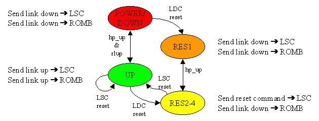
Figure 2. LDC Power-up and Reset state machine
LDC powers up in POWER/DOWN state. Here the LDC waits for hw_ok and
rlup, and is continuously sending link down command to the LSC. By doing
this, it is assured that LDC will come up before the LSC in power up sequence,
and no data written to LSC will be lost. When the LDC is in UP state, a
LSC reset will do nothing to the state machine, but CRC error latches and
Test mode state is cleared.
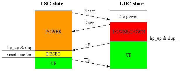
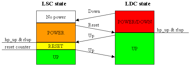
In case the LDC is powered down and powered up again during normal operation, a reset in any of the cards MUST be made. Otherwise, they will both stay in state down. If the LSC is powered down and powered up again, the link will recover by itself.
For simulation with software user can select via the generic SIMULATE
(to choose simulation parameters set to 1) a shorter filter length (5 bits),
in order to increase simulation speed. Normal initialization time on each
card is 25 ms., for simulation reduced to 6µs.
The user can select several parameters of the card through the following
generics:
| Generic name | Description | Valid values | Included in LSC | Included in LDC |
| SIMULATE |
|
1 = ON (25 ms init.time) . 0 = OFF( 6 µs init. time) |
|
YES |
| LCLK_FREQ |
|
1 = 62.5 MHz LCLK clock 0 = 40 MHz LCLK clock | NO | YES |
| ACTIVITY_LENGTH | Activity_led stays illuminated after write operation for 2^(ACTIVITY_LENGTH) clock cycles | Integer | YES | YES |
| FIFODEPTH | Depth of FIFO | Integer (max. 512 for EP20K30ETC144 ) | YES | YES |
| LOG2DEPTH | Log2(FIFODEPTH) | Log2(FIFODEPTH) | YES | YES |
| FULLMARGIN | Number of words that must be free in the FIFO before setting flow control. | <FIFODEPTH | YES | YES |
Table 7: HOLA generics.
for the current implementation, values are as follows:
| Generic name | LSC | LDC |
| SIMULATE | 0 | 0 |
| LCLK_FREQ | - | 0 |
| ACTIVITY_LENGTH | 6 | 6 |
| FIFODEPTH | 64 | 512 |
| LOG2DEPTH | 6 | 9 |
| FULLMARGIN | 32 | 256 |
With these values, the LSC can accept up to 32 words (FIFODEPTH-FULLMARGIN) after LFF# was asserted.
These are the different PCB mounting options for the source and destination
cards:
| R16 | R17 | R18 | CP2 | |
| LSC | - | 200 | 200 | OPEN |
| LDC | 0 | - | - | FILL |
Table 9: Mounting table
Transmitter Interface
The transmitter section validates incoming 16-bit wide data (TXD [0:15]) on the rising edge of the GTX_CLK. That incoming data is then 8-bit/10-bit encoded, serialized, and transmitted sequentially over the differential high-speed I/O channel. The clock multiplier multiplies the reference clock (GTX_CLK) by a factor of 10, creating a bit clock. This internal bit clock is fed to the parallel-to-serial shift register. This register transmits data on both edges of the bit clock, providing serial data at a rate of 20 times the reference clock.
An 8-bit/10-bit encoding algorithm is implemented in the transmitter
section of the device; it?s the same algorithm used by fiber channel and
the gigabit Ethernet. The decoding is transparent to the user; data is
internally encoded such that the user only has to write 16-bit data. The
8-bit/10-bit encoder converts 8-bit wide incoming data to a 10-bit wide
encoded data character. This is done to improve its transmission characteristics.
The encoding scheme maintains the signal DC balance by keeping the number
of ones and zeros the same. This provides good transition density for clock
recovery and improves error checking.
Externally, the device has a 16-bit wide interface; internally, the
data is split into two 8-bit wide bytes for encoding. Each byte is fed
into a separate encoder. The encoding is dependent upon two additional
input signals, the TX_EN and TX_ER. Tabl e 1 provides the transmit data
control decoding.
| TX_EN | TX_ER | ENCODED 20 BIT OUTPUT |
| 0 | 0 | IDLE(<K28.5,D5.6> or <K28.5,D16.2>) |
| 0 | 1 | Carrier Extend (K23.7,K23.7) |
| 1 | 0 | Normal data character |
| 1 | 1 | Transmit error propagation (K30.7,K30.7) |
Receiver Interface
The receiver section accepts 8-bit/10-bit encoded differential serial
data. The interpolator and clock recovery circuit lock to the data stream
and extract the bit rate clock. This recovered clock is used to re-time
the input data stream. The serial data is then clocked into the serial-to-parallel
shift registers. The 10-bit wide parallel data is then multiplexed and
fed into two separate 8-bit/10-bit decoders, where the data is then synchronized
to the incoming data steam word boundary by detection of the K28.5 synchronization
pattern.
| RX_DV/LOS | RX_ER | ENCODED 20 BIT OUTPUT |
| 0 | 0 | IDLE(<K28.5,D5.6> or <K28.5,D16.2>) |
| 0 | 1 | Carrier Extend (K23.7,K23.7) |
| 1 | 0 | Normal data character |
| 1 | 1 | Transmit error propagation (K30.7,K30.7) |
The by the S-LINK specified two words after LFF# being asserted become, for the current implementation, 32 words. This value can be set by the user means the generics FIFODEPTH and FULLMARGIN previously described.
Architecture of the HOLA LSC Card
Data coming from the return channel is read at the positive edges of RXCLK, the recovered return channel clock. No FIFO is required for them.
HOLA LSC provides two additional LEDs. ACTIVITY_LED, illuminated when
a write operation was performed on the FIFO in the previous 2^ACTIVITY_LENGTH
cycles (with ACTIVITY_LENGTH being the generic described in Tables 7 and 8),
and DERRLED_N, to show that the input FIFO is COMPLETELY full, and
no more data will be accepted (if this LED is illuminated, there is an
error as the user violated the S-LINK specification by sending more than 32 words after LFF# got
asserted).
| Clock | Functions | Speed |
| UCLCK | Clock from FEMB -> Write in FIFO | Typ. 40 MHz |
| ICLK | Internal clock ->Read from FIFO, any internal logic | 62.5 MHz |
| GTX_CLK | Clock for the serialization for Forward Channel, multiplexing | 125 MHz |
| RX_CLK | Recovered clock from Return Channel | 125 MHz |
The timing parameters for the LSC are listed in Table 13:
| Symbol | Description | Min | Max | Units |
| tDS | Data Set-up time | 10 | ns | |
| tDH | Data Hold time | 1 | ns | |
| tENS | Enable Set-up time | 10 | ns | |
| tENH | Enable Hold time | 1 | ns | |
| tWFF | Write Clock to Full Flag | 12 | ns | |
| tCLK | Clock Cycle time | 25 | ns | |
| tCH | Clock High time | 11 | ns | |
| tcl | Clock Low time | 11 | ns |
The 16-bit serial data received on the LDC is first decoded by the TLK2501, and converted into a 16-bit parallel output (working at 125 MHz).32-bit data must be then written to the FIFO (this operation is made at 62.5 MHz). This conversion is made via a 'demultiplexor', which simply latches the MSB until the next clock cycle, where the LSB is received. The 32-bit word is the written to the FIFO at 62.5 MHz.
At the positive edges of the LCLK clock (typically 40 MHz), a 32-bit word is read from the FIFO and transmitted to the ROMB. Note that in the FIFO 'write' is a 16-bit operation, but 'read' a 32-bit one.
Architecture of the HOLA LDC Card
Words in the return channel are written at the positive edges of XCLK,
the internal 125 MHz clock.
| Clock | Functions | Speed |
| RX_CLK | Clock for the serializer/deserializer and demultiplexer | 125 MHz |
| LCLK | Clock for LD -> Read from FIFO | Typ. 40 MHz |
| ICLK_2 | Clock for the internal logic and write to FIFO | 62.5 MHz |
| GTX_CLK | Clock for the return channel | 125 MHz |
Block front writes the data received from the deserialiser to
the FIFO. To guarantee the maximum set up and hold times data will registered
always in the high-to-low transition of the internal clock ICLK_2. The
internal 16-bit register datamsb is used to take the MSB data received
first. In case it is necessary to wait for one clock cycle to give the
data to the FIFO, LSB data will be kept in the 16-bit register datalsb.
A timing diagram is shown in the following figure.
Table 15 gives the guaranteed timing parameters for LDC. The suffix
-40 is used for the parameters of the 40 MHz LCLK version, suffix -625
is used for the 62.5 MHz LCLK version.
| Symbol | Description | Min | Max | Units |
| tDS | Data Set-up time | 10 | ns | |
| tDH | Data Hold time | 1 | ns | |
| tENS | Enable Set-up time | 10 | ns | |
| tENH | Enable Hold time | 1 | ns | |
| tWFF | Write Clock to Full Flag | 12 | ns | |
| tCLK-40 | Clock Cycle time | 25 | ns | |
| tCH-40 | Clock High time | 11 | ns | |
| tCL- 40 | Clock Low time | 11 | ns | |
| tCLK-625 | Clock Cycle timetCL | 16 | ns | |
| tCH-625 | Clock High time | 7 | ns | |
| tCL- 625 | Clock Low time | 7 | ns |
| Min | Typ | Max | Units | |
| LSC - 40 MHz UCLK clock
LDC - 40 MHz LCLK clock |
2805 | 3300 | 4290 | mW |
| LSC - 40 MHz UCLK clock
LDC - 62.5 MHz LCLK clock |
- | - | - | mW |
Power consumption of the Altera device can be estimated by inserting the .pwf files generated after simulation in the Quartus software, and performing there again a timing simulation. In the simulator settings it must be added the .pwf as "Source of Vector Stimuli", and in Simulator Settings the option "Estimate power consumption" must be also selected.
The results (and a comparison with the results obtained using the APEX
power consumption calculator are shown below).
| Quartus estimation | APEX power calculator estimation | |||||
| Internal power (mW) | IO power(mW) | Total(mW) | Internal power(mW) | IO power(mW) | Total(mW) | |
| LDC - 62.5 MHz LCLK clock | 301.2 | 0.024 | 301.24 | 301.83 | 34.99 | 336.82 |
| LDC - 40 MHz LCLK clock | 265.66 | 0.016 | 265.67 | 228.09 | 28.14 | 256.23 |
| LSC - 62.5 MHz input clock | - | - | - | 307.1 | 20.82 | 327.92 |
| LSC - 40 MHz input clock | 301.7 | 0.036 | 301.74 | 307.1 | 19.07 | 326.16 |
Table 15: Simulated Altera power consumption
The estimation using the APEX power calculator will be less accurate, since the calculation was done for all flip-flops (773 for the LDC, 735 for the LSC) and LEs (111 ESBTON and 763 ESBTOFF for the LDC, 86 and 789 for the LSC) assigned to a 62.5 MHz clock (or a 40 MHz clock in the case of LDC with 40 MHz LCLK clock. LSC is always calculated at 62.5 MHz because most of the registers will be working at that speed independently of the input clock). In the reality there will be an amount of registers running at others speeds.
Other sources of power consumption are the SerDes and the optical transceiver. According to the values from their datasheets, the TLK2501 consumes 360 mW for a data rate of 2.5 Gbps. For the optical transceiver power consumption is 412 mW. The 2.5V for the SerDes will be generated out of 3.3V with a drop-down converter. Its actually power consumptio will be then 475 mW.
For the moment the S-Link VHDL model only allows input clocks at 40 MHz.