1. Introduction
The ODIN S-LINK is a standard duplex S-LINK that uses the low power G-Link chip-set (HDMP-1032/34) as physical layer. Its components are the Link Source (LSC), the Link Destination (LDC) cards and a fiber optic cable with Volition duplex connectors. More information, including this document, about the ODIN Interface can be found on the World Wide Web at:
The reader of this document should know the basics of the S-LINK specification. This data sheet only point out a few important features of ODIN and makes a few clarifications. The S-Link specification can be downloaded from the Worldwide Web at:
2. Main Features
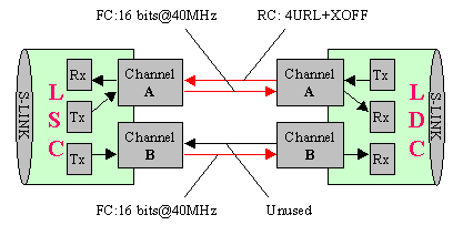
ODIN exists in two different operation versions, single and double channel, where one or two G-Link chip sets are used in the forward channel. These two versions cannot be mixed; i.e. a single channel LSC will not work with a double channel LDC and vice versa. ODIN also exists in two different voltage versions, 3.3V and 5V. See figure 2-1 for block diagram of the double channel version and the usage of the two optical fibers.
The S-LINK code for the ODIN cards is:
The main features of the ODIN S-LINK implementation are:
General features
Fix the ODIN S-LINK cards with screws to standoff pillars and front panel mounting holes to avoid mechanical stress and contact problems. For proper operation the board should be fixed by all four screws. Avoid mechanical stress on the cards during mounting. Do not plug in and out the cards on the motherboard when this is powered on.
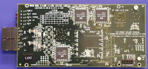
Before powering up, check that the voltage version of the ODIN is the same as the motherboard. 5V motherboard should have a voltage keying pin described in S-LINK specification [1] and the 3.3V ODIN should not have a voltage hole to eliminate the chance of mounting 3.3V S-LINK on a 5V motherboard. Mounting 5V ODIN on a 3.3V motherboard is physically possible, but will not work.
Double ODIN features two optical connectors, marked A and B, and cables must not be switched. Maximum length difference is 1 meter. If cables are different in length channel B should have the shorter cable for better word alignment tolerance.
Connect the optical fiber(s) and after powering up the cards the link goes up immediately and Power and Link up leds go on. There is no need for a reset at power up as the cards go up when powered on and fibers are connected.
4. Operating Conditions
| Symbol | Description | Min | Typical | Max. | Units |
| Icc,d | Current drawn, single ODIN | 700 | 1000 | 1200 | mA |
| Icc,d | Current drawn, double ODIN | 1000 | 1200 | 1400 | mA |
| Vcc (3.3V board) | Voltage | 3.1 | 3.3 | 3.5 | V |
| Vcc (5V board) | Voltage | 4.5 | 5.0 | 6.0 | V |
| Top | Temperature | 0 | 25 | 70 | C |
Table 5-1 gives the required timing parameter for LSC for proper operation.
See [1] for explanation of the parameters.
| Symbol | Description | Min | Max | Units |
| tDS | Data Set-up time | 10 | ns | |
| tDH | Data Hold time | 1 | ns | |
| tENS | Enable Set-up time | 10 | ns | |
| tENH | Enable Hold time | 1 | ns | |
| tWFF | Write Clock to Full Flag | 12 | ns | |
| tCLK | Clock Cycle time | 25 | ns | |
| tCH | Clock High time | 11 | ns | |
| tcl | Clock Low time | 11 | ns |
| Symbol | Description | Min | Max | Units |
| tDS | Data Set-up time | 10 | ns | |
| tDH | Data Hold time | 1 | ns | |
| tENS | Enable Set-up time | 10 | ns | |
| tENH | Enable Hold time | 1 | ns | |
| tWFF | Write Clock to Full Flag | 12 | ns | |
| tCLK-single | Clock Cycle time | 31 | ns | |
| tCH-single | Clock High time | 13 | ns | |
| tCL-single | Clock Low time | 13 | ns | |
| tCLK-double | Clock Cycle time | 25 | ns | |
| tCH- double | Clock High time | 11 | ns | |
| tCL-double | Clock Low time | 11 | ns |
6. Optical characteristics
| Symbol | Description | Min | Typical | Max. | Units |
| Link length (50/125 microns) | 2 | 550 | m | ||
| Link length (62.5/125 microns) | 2 | 260 | m | ||
| BER | Bit Error Rate | 10-12 | |||
| lambda | Center wavelength | 830 | 850 | 860 | nm |
| LED symbol | Color | Function at LSC | Function at LDC |
| PWR | green | Power On | Power On |
| TST | red | Self test Mode | Self test Mode |
| ERR | red | - | Data Error |
| UP | green | Link Up | Link Up |
| XOF | red | Link Full Flag | Flow control active |
The UDW input lines are unused. If ODIN is set to 16 or 8-bit mode the effective transmission rate will go down accordingly since all 32 bits always are transferred.
9. Data Transfer
The ODIN S-LINK will transer all input data when up, Power and Link Up leds are on and LDOWN# lines are high on both sides. If data is written to single channel LSC faster than 32 MHz the LFF# flag will go low and the XOFF led goes on at the LSC, even if there is no flow control sent from LDC. This is because maximum data transmission rate is 128 Mbytes/s. For maximum transfer rate, 2 more words should be written to LSC after LFF# goes low.
For small data block sizes the LFF# line will also become active as error detection and S-LINK control words take up bandwidth. Figure 9-1 gives maximum average transfer rate for small block sizes. The block size refers to the ATLAS event data format where one Begin of Fragment control word and one End of Fragment control word frames the data words. These transfer rates given are maximum values and to reach the maximum value 2 more words must be written to LSC after LFF# goes low. Also note that the graph shows the average values while the nominal value inside a block is the maximum transfer rate.
10. S-LINK Reset
ODIN S-LINK features an improved reset protocol, which is backward compatible. The user may reset the whole link from either side, or even both sides. The card reset is changed into a link reset to make the reset an easy and reliable operation regardless of usage.
If the link is down prior to the reset cycle, LDC will come up before LSC, regardless of which side the reset is performed. This eliminates the chance of data written to LSC being lost because of LDC being down.
If the link is up prior to the reset cycle, the card where URESET# line is asserted will go down according to [1]. The other side will be reset without going down.
It is not recommended to perform a reset while writing data to the LSC, as this will cause data loss.
11. Test Mode
Self-test mode fully complies with S-LINK specification. UTDO# line is sampled at link reset.
12. Flow Control
The Read out buffer size can be calculated from the formula given in [1]:
Where:
RBS = Read out Buffer size (words)
LDCrt = LDC reaction time to send XOFF after UXOFF# goes
low (ns).
LSCrt = LSC reaction time to stop transmitting data after
XOFF received (ns).
L = Length of S-LINK (m).
UFD = Unit Fibre Delay - time for light to travel 1m in fibre (approx.
6 ns/m).
DTR = Data Transfer Rate (ns/word).
Data words in LSC and LDC pipelines are included in LSCrt
and LDCrt respectively.
| Symbol | Single ODIN | Double ODIN |
| LDCrt | 350 | 550 |
| LSCrt | 200 | 300 |
| UFD | 6 | 6 |
| DTR | 31.25 | 25 |
Return Lines are functional during data transfer and int test modes. LRL[3..0] lines will stay unaltered when the link is down. An internal parity checking logic ensures proper operation of the Return Lines. The sampling rate of the return lines is 8 MHz for the single channel version and 5 MHz for the double channel version.
14. Error Detection
ODIN features a CRC-based block error detection and errors are reported in the following control word, as specified in [1]. There is also a weak word-by-word error detection, but this only looks at the internal data format and G-Link error bit, and does not look at the actual data
S-LINK control words uses parity bits as error detection in order to separate data errors from control word errors.
15. Link Down Function
The following events may result the link down signal to be asserted:
1. Reset cycle
2. Self-test mode
3. Local reset, i.e. the LDOWN# is asserted only on the card where
URESET# is set low.
4. LSC or LDC is not powered up
5. Broken optical link
6. Fatal error occurred
The three first cases are covered by the S-LINK specifications. In the other cases the link down should be latched until a reset cycle. This is true except on LSC power down as the LSC is powered up in a reset state. On LDC power down, LSC will go down caused by the return channel loosing synchronization. This link down state will be latched until cleared by a reset at either side.
16. Known Bugs
For UCLK in low MHz range, <10 MHz, flow control does not work in Test Mode, as this sometimes will cause a link down. Going out of test mode and perform a link reset clears this state.
References
[1]. O. Boyle, R. McLaren, E. van der Bij, "The S-LINK Interface
Specification",
http://www.cern.ch/HSI/s-link/spec/spec/
CERN, 1997.