CERN ECP-Division, EDU/DQ Section
Erik van der Bij
23 July 1997
The Simple S-LINK to PMC (SSP) interface is a PCI Mezzanine Card that is needed to interface S-LINK Link Destination Cards (LDCs) in a PMC environment. The interface itself is fully compliant to the PMC as well as the S-LINK specification. However, when the S-LINK LDC is plugged onto the SSP, the total height will be larger than allowed by the PMC specification.
The interface was made with simplicity of design in mind. This has consequences for the ease of programming only. With the integrated DMA, the board can transfer data at the full PMC bus speed which is theoretically 130 MByte/sec.
The Simple S-LINK to PMC interface has Read-out Motherboard (ROMB) functionality, is a duplex implementation, which can handle an LCLK with a frequency up to 33 MHz, having 5 Volt signal levels and a maximum transfer rate of 130 MByte/sec. In S-LINK terms this is coded as a ROMB-D-33-x-5.0-130.
Furthermore the interface features:
As far as the PMC interface goes it features:
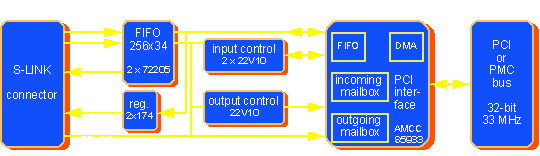
Figure 1 shows a block diagram of the board. The hardware is based on the S5933 PCI controller from the company Applied Micro Circuits Corporation (AMCC). It is this chip that implements the PCI functionality, the DMA interface and access to mailbox registers that control the S-LINK. The S5933 furthermore incorporates several internal registers that provide control and status of the chip itself.
Figure 1: block diagram of the Simple PMC to S-LINK interface
To set up the S-LINK, outgoing mailbox register 1 is used. With this register the data width, reset, user test data out and return lines can be set.
Data received from the S-LINK will first be stored in a pair of FIFO chips, which we'll call the "External FIFO". The input control chip will move the data from this External FIFO to the FIFO that is inside the S5933. This latter chip we'll call "AMCC FIFO". You will know from reading the Bus Master Control/Status register (MCSR) on the S5933 if there is actually data in the AMCC FIFO. The data may be read from the AMCC FIFO by doing single reads, or the interface can itself transfer the data to external memory by using the DMA that is built in the S5933. For this the DMA should be enabled by writing to the MCSR. When after that the transfer address and the length of the transfer are set, the DMA will automatically transfer all data from the AMCC FIFO, which then will be transferred to the memory. Whenever both the External FIFO and the AMCC FIFO are emptied, the DMA will be suspended. It will continue again when the S-LINK transfers more data. It is possible to let the S5933 generate an interrupt when the DMA is finished, but not when it is suspended.
To handle words with LCTRL# active or words with the LDERR# line active, a simple mechanism is used. You have to write to the outgoing mailbox register 1 the value of LCTRL# and LDERR# that you expect. The input control logic will only transfer data from the External FIFO to the AMCC FIFO when the actual values of LCTRL# and LDERR# correspond to those set in the mailbox register after which you may read from incoming mailbox register 4, byte 3 the actual values of the next word. That means that if there is no data in the AMCC FIFO, it can be caused by either of two reasons:
You may differentiate between them by comparing the mailbox register values. Only if LCTRL#, LDERR# or LDOWN# change value, the incoming mailbox register 4, byte 3 will be written with the new values. The S5933 can be programmed to generate a PMC interrupt on this event.
The interface will assert the UXOFF# line to the S-LINK if the External FIFO is half full. I.e. the S-LINK may send 128 words before it will see UXOFF# asserted. After that, there is still space for another 128 words before the External FIFO would overflow.
The Simple S-LINK to PMC interface is a standard PMC board and can be mounted with the standard PMC mounting screws. Before mounting it on the motherboard, you should mount the S-LINK Link Destination Card with the appropriate screws in the holes foreseen for this purpose.
All accesses to the Simple S-LINK to PMC interface are done via the AMCC S5933 PCI controller chip. It is this chip that needs to be set up for the correct type of PCI accesses with the PCI Configuration Space Registers that are described in the PCI specification and in the AMCC S5933 databook. All accesses to the S-LINK go via the PCI Operation Registers of which the description can be found in the AMCC S5933 databook.
The PCI configuration registers are the standard registers that every PCI compatible card has. Detailed information on the usage of those registers can be found in the PCI Specification and in the AMCC S5933 databook.
Register name : Vendor Identification
Address offset: 00-01h
Boot-load     : 10DCh (CERN)
Attribute     : Read Only (RO)
Size          : 16 bits
Register name : Device Identification
Address offset: 02-03h
Boot-load     : 0011h (Simple S-LINK to PMC interface)
Attribute     : Read Only (RO)
Size          : 16 bits
Register name : PCI Command
Address offset: 04-05h
Boot-load     : 0000h
Attribute     : Read/Write (R/W on 6 bits, Read Only on all others)
Size          : 16 bits
Register name : PCI Status
Address offset: 06-07h
Boot-load     : 0080h
Attribute     : Read Only (RO), Read/Write Clear (R/WC)
Size          : 16 bits
Register name : Revision Identification
Address offset: 08h
Boot-load     : 00h
Attribute     : Read Only (RO)
Size          : 8 bits
Register name : Class Code
Address offset: 09-0Bh
Boot-load     : 028000h     (network controller/
                           other communication device/
                           programming interface 00h)
Attribute     : Read Only (RO)
Size          : 24 bits
Register name : Cache Line Size
Address offset: 0Ch
Boot-load     : 00h
Attribute     : Read Only (RO)
Size          : 8 bits
Register name : Latency Timer
Address offset: 0Dh
Boot-load     : F8h
Attribute     : Read/Write bits 7:3; Read Only bits 2:0
Size          : 8 bits
Register name : Header Type
Address offset: 0Eh
Boot-load     : 00h (Single function device, Format field 0)
Attribute     : Read Only (RO)
Size          : 8 bits
Register name : Built-in Self-test
Address offset: 0Fh
Boot-load     : 00h
Attribute     : D7, D5-0 Read Only, D6 as PCI bus write only
Size          : 8 bits
Register name : Base Address 0
Address offset: 10h
Boot-load     : FFFFFFC0h (64 bytes in memory space)
Attribute     : High bits Read/Write; low bits Read Only
Size          : 32 bits
Register name : Base Address 1-5
Address offset: 14h, 18h, 1Ch, 20h, 24h
Boot-load     : 00000000h (disabled)
Attribute     : High bits Read/Write; low bits Read Only
Size          : 32 bits
Register name : Expansion ROM Base Address
Address offset: 30h
Boot-load     : 00000000h (disabled)
Attribute     : bits 31:11, bit 0 Read/Write; bits 10:1 Read Only
Size          : 32 bits
Register name : Interrupt Line
Address offset: 3Ch
Boot-load     : FFh (unknown)
Attribute     : Read/Write
Size          : 8 bits
Register name : Interrupt Pin
Address offset: 3Dh
Boot-load     : 01h (INTA#)
Attribute     : Read Only (RO)
Size          : 8 bits
Register name : Minimum Grant
Address offset: 3Eh
Boot-load     : 00h (no stringent requirement)
Attribute     : Read Only (RO)
Size          : 8 bits
Register name : Maximum Latency
Address offset: 3Fh
Boot-load     : 00h (no stringent requirement)
Attribute     : Read Only (RO)
Size          : 8 bits
The PCI operation registers are the registers inside the AMCC S5933 chip. All accesses to the S-LINK are done via those registers. Those registers are mapped into the PCI memory space, the base address of them can be found in the PCI configuration space in Base Address Register 0.
The following section describes how the operation registers are used in the interface. Detailed information on the usage of those registers can be found the AMCC S5933 databook.
Register name : Outgoing Mailbox 1
Address offset: 00h
Boot-load     : XXXXXXXXh
Attribute     : Read/Write
Size          : 32 bits
Bit assignment: bit 31-26: not used
                bit 25   : EXPLCTRL#  (0=control word, 1=data word)
                bit 24   : EXPLDERR#  (0=error, 1=no error)
                bit 23-12: not used
                bit 11   : URL3
                bit 10   : URL2
                bit  9   : URL1
                bit  8   : URL0
                bit  7- 5: not used
                bit  4   : UDW1     ([UDW1,UDW0]: [00]=32-bit, [01]=16-bit, [10]=8-bit, [11]=reserved)
                bit  3   : UDW0
                bit  2   : URESET#  (0=reset, 1=normal operation, see protocol with LDOWN#)
                bit  1   : UTDO#    (0=test data output, 1=test data not output)
                bit  0   : FRESET#  (0=reset external FIFO, 1=normal operation)

Description:
The Outgoing Mailbox Register is read by the interface on a regular basis (about every microsecond), so you have to take into account a certain delay before any changes are seen. Note that bits of the same functional group are put together in one byte. If you need to change only bits within one group, you may make use of that to prevent any bit masking operations by doing byte access instead of word accesses of the register.
Bits 11 to 8 and bits 4 to 1 of this register are connected to the corresponding pins of the S-LINK interface and have the functionality as described in the S-LINK specification.
Bit 0, FRESET# resets the External FIFO on the board. For the interface to work correctly, the External FIFO should be reset once after power-up by writing a 0 to this bit. For normal operation this bit should be set to 1. If this bit is 0, the External FIFO is kept reset, which means that no data will be stored. The UXOFF# line to the LDC will be 1 during this, which makes that the interface will effectively sink data at full speed. Refer to section 4.2 for a description of the reset procedure.
Bit 25 and 24 are the values of LCTRL# and LDERR# that you expect to receive from the LDC. If a dataword is being read out of the External FIFO that has LCTRL# and/or LDERR# values that are different than those in the outgoing mailbox register 1, the input control logic will not transfer it to the AMCC FIFO. The actual values of LCTRL# and LDERR# of this last, different dataword (that is read out from the External FIFO, but not written into the AMCC FIFO) can be read from incoming mailbox register 4, byte 3. To continue the transfer, you will have to copy those values to corresponding bits in the outgoing mailbox register 1.
Only if LCTRL#, LDERR# or LDOWN# change value, the incoming mailbox register 4, byte 3 will be written with the new values. The S5933 can be programmed to generate a PMC interrupt on this event.
Register name : Outgoing Mailbox 2-4
Address offset: 04h, 08h, 0Ch
Boot-load     : XXXXXXXXh
Attribute     : Read/Write
Size          : 32 bits
Description   : those registers have no functionality
Register name : Incoming Mailbox Register 1-3
Address offset: 10h, 14h, 18h
Boot-load     : XXXXXXXXh
Attribute     : Read Only (RO)
Size          : 32 bits
Description   : those registers have no functionality
Register name : Incoming Mailbox Register 4
Address offset: 1Ch
Boot-load     : XXXXXXXXh
Attribute     : Read Only (RO)
Size          : 32 bits
Bit assignment: bit 31-28: read always 0
                bit 27   : OVFLW  (0=normal, 1=overflow occurred)
                bit 26   : LDOWN# (0=link down, 1=link up)
                bit 25   : LCTRL# (0=control word, 1=data word)
                bit 24   : LDERR# (0=error, 1=no error)
                bit 23-0 : undefined
Description:
Bit 27 (OVFLW) will be set when the External FIFO is overflown. This may only happen when a simplex LDC is connected to the Simple S-LINK to PMC interface and data is received faster by the LDC than the interface can handle. When a duplex LDC is used, the flow control mechanism should prevent an External FIFO overflow from happening. When bit 27 is set, the interface will continue to work, but data may be lost. Once set, the bit can only be cleared by resetting the interface via the Bus Master Control/Status Register (MCSR).
Bit 26 (LDOWN#) in this register is connected to the corresponding line on the S-LINK connector. If a change that is stable for more than two PCI clock periods (about 60 nsec), occurs on this line, the new value will be written to the Incoming Mailbox Register 4, byte 3. You may use this event to generate an interrupt by setting up the Interrupt Control/Status Register (INTCSR). You may as well check if a new value is written by reading the Mailbox Empty/Full Status Register (MBEF), bit 31.
When the values of LCTRL# and LDERR# from the last dataword that is read out of the External FIFO do not correspond to those as set in the Outgoing Mailbox Register 1, bits EXPLCTRL# and EXPLDERR#, the interface will not transfer it to the AMCC FIFO. It will write the new values of LCTRL# and LDERR# in the Incoming Mailbox Register 4 and wait until you write the same values back in the corresponding bits of the Outgoing Mailbox Register 1 before filling the AMCC FIFO. You may use the event that the Incoming Mailbox Register 4, byte 3 is written to generate an interrupt by setting up the Interrupt Control/Status Register (INTCSR). You may also check if a new value is written by looking at the Mailbox Empty/Full Status Register (MBEF), bit 31.
This mechanism makes that all words you read from the AMCC FIFO until it is empty, have the values of LCTRL# and LDERR# that you have written to the Outgoing Mailbox Register 1.
Note that at power on, the IMB4 register is written with the current values at that moment. However, the status in the MBEF will not indicate that the register is written. When you reset the card via the Bus Master Control/Status Register (MCSR), the IMB4 will be written with the current values and the MBEF will be updated correctly.
Register name : FIFO Port
Address offset: 20h
Boot-load     : XXXXXXXXh
Attribute     : Read Only (RO)
Size          : 32 bits
Bit assignment: bit 31-0: LD[31..0]
Description:
The FIFO Register Port, which is in fact the AMCC FIFO, contains the values of the Link Data lines received from the LDC. The value of the LDCTRL# and LDERR# bits that come along with each dataword are the ones that you have written into the Outgoing Mailbox Register 1. Please read a description of the Outgoing Mailbox Register 1 on the functioning of those bits.
Register name : Master Write Address
Address offset: 24h
Boot-load     : 00000000h
Attribute     : Read/Write
Size          : 32 bits
Description   : see AMCC S5933 databook
Register name : Master Write Transfer Count
Address offset: 28h
Boot-load     : 00000000h
Attribute     : Read/Write
Size          : 32 bits
Description   : see AMCC S5933 databook
Register name : Master Read Address
Address offset: 2Ch
Boot-load     : 00000000h
Attribute     : Read/Write
Size          : 32 bits
Description   : this register has no functionality
Register name : Master Read Transfer Count
Address offset: 30h
Boot-load     : 00000000h
Attribute     : Read/Write
Size          : 32 bits
Description   : this register has no functionality
Register name : Mailbox Empty/Full
Address offset: 34h
Boot-load     : 00000000h
Attribute     : Read Only (RO)
Size          : 32 bits
Description   : see AMCC S5933 databook
Register name : Interrupt Control/Status
Address offset: 38h
Boot-load     : 00000000
Attribute     : Read/Write (R/W), Read/Write_One_Clear Only (R/WC)
Size          : 32 bits
Description   : see AMCC S5933 databook
Register name : Bus Master Control/Status
Address offset: 3Ch
Boot-load     : 000000E6h
Attribute     : Read/Write, Read Only, Write Only
Size          : 32 bits
Bit assignment: bit 24    : interface logic reset  (0=normal operation, 1=reset)
                other bits: see AMCC S5933 databook
Description:
Writing a 1 to bit 24 resets the logic on the interface. This does not influence the values that are taken from the Outgoing Mailbox Register 1, nor will the External FIFO be emptied. For the interface to work, bit 24 must be reset to 0. After removing of the reset, Incoming Mailbox 4 will be written and the MBEF register will be updated accordingly. Note that for the interface to work, the External FIFO should be reset once after power-up. This can be done via the bit FRESET# in the Outgoing Mailbox Register 1 (OMB1). Refer to section 4.2 for a description of the reset procedure.
For the functionality of the other bits of the MCSR, please refer to the AMCC S5933 databook
The previous sections have described the basic functions of the many registers the Simple S-LINK to PMC interface contains. The following sections will give the user some extra information on how to program the device in an optimal way. First it will be described how the PCI interface must be set up. This is followed by sections that explains how to transfer data efficiently and how to handle the return lines and link down status changes.
When the host computer where the interface is plugged into, it will have automatically configured the PCI Configuration Registers. Normally there is no need to change any of the values to let the interface operate correctly. You should check the Vendor Identification and Device Identification registers to make sure that the right interface is plugged in.
After that, you should read back the Base Address 0 register to find where the host computer has located the interface in the memory space. The interface will occupy 16 words in total.
After power-up, the External FIFO, the add-on logic and the AMCC FIFO on the board should be reset once to make the interface work correctly. To correctly reset the interface, the following steps have to be made in the right order:
This translates into the more detailed pseudo code:
A one clock cycle delay between each of those writes is enough.
Before any transfer can be done, the Link Destination Card lines must be set up. I.e. the value for URL[3..0], UDW[1..0], URESET# and UTDO# must be set correctly. This can be done by writing to the Outgoing Mailbox Register 1 (OMB1). Also you must write the expected values for LCTRL# and LDERR# in this register. Normally the values for those would be LCTRL#=0 and LDERR#=1, as the first word received will in most cases be a control word without an error. It will take up to 1 µsec before the new value written to the OMB1 is seen. You may check the Mailbox Empty/Full Status Register (MBEF) to check if the value indeed is read by the interface. If it does not get read, it means that there is a hardware problem.
To make sure you don't get any spurious data with unknown LCTRL# and LDERR# values, you might keep the External FIFO reset until the above setup of the Outgoing Mailbox Register 1 is done.
To reset the Link Destination Card, the protocol between URESET# and LDOWN# as described in the S-LINK specification should be implemented:
This is in more detailed pseudo code:
Note that the reset of the interface with the FIFOs as described in section 4.2.1 has to be done once only. The reset of the Link Destination Card will be needed every time the link has gone down (LDOWN# has gone to 0). Note that on a duplex link, every time a reset is done on one side of the link, also the other side of the link should be reset.
For the actual data transfer, you have the option of reading data under processor control or by DMA. For single reads under processor control, you first have to check if there is data in the AMCC FIFO before reading it. Note that a PCI Initiator may not perform burst accesses from the AMCC FIFO (see section 10.2.1 of the AMCC databook). For those two reasons, this type of transfer will be relatively slow.
For fast data transfers, you may use the built in DMA engine. This has the advantage that there is no need to check the AMCC FIFO status before doing the transfer, as the DMA will stop itself if the AMCC FIFO is empty and will resume automatically when there is again data available. You may enable the DMA by setting up the Bus Master Control/Status Register (MCSR). After that you only have to write the Master Write Address and Transfer Count registers to let the DMA start. You may set up the interface that it will generate a PMC interrupt when the DMA is finished. Please refer to Chapter 10 of the AMCC databook.
Note that the value of UCTRL# and LDERR# for all words received should be the same as what was written to the Outgoing Mailbox Register 1 for the whole DMA transfer. If any word that has different values for those bits is received from the LDC, the S5933 will not be filled and the transfer will stop once the AMCC FIFO is empty. You may trigger an interrupt on this event as it will cause the Incoming Mailbox Register 4 to be written. After that you must read the new value for UCTRL# and LDERR# from the Incoming Mailbox Register 4 and write those values back into the Outgoing Mailbox Register 1 and the transfer will continue. Before you write IMB4, you have to check that the AMCC FIFO indeed is empty as otherwise you may interpret those as having the new values for UCTRL# and LDERR#.
In case a 16-bit or 8-bit Link Destination Card is connected to the board, the interface will only use LD[15..0] or LD[7..0] respectively. This makes that bits LD[31..16] or LD[31..8] are not used. The DMA transfers however, will always be 32-bit transfers, which means that it is not possible to use the DMA if you want to transfer a block of consecutive datawords to the memory with 16-bit or 8-bit Link Destination Cards.
You must be very careful in the order of instructions that check if the AMCC FIFO is empty and that check if the values of LCTRL# and LDERR# in the Incoming Mailbox register 4 (IMB4) have changed.
Let's give an example.
Assume that after reset you had set up the interface to receive control
words without errors (by writing a 0 to the EXPLCTRL# bit and a 1 in the
EXPLDERR# bit in the OMB1). The S-LINK is idle, so you are not receiving
any words. If there is no data in the AMCC FIFO, it can be because of two
reasons:
Your program cannot directly distinguish between those two cases. Therefore your program will poll the AMCC FIFO empty bit to see if data has arrived, and if it hasn't, it will check the values of LCTRL# and LDERR# in the IMB4 to see if data has arrived with those bit different than set in OMB1. It will loop doing those two checks (although also interrupts for those events may be set up).
If at a certain moment the S-LINK sends a control word, immediately followed by a dataword, the hardware will do the following:
Those two things happen very quickly after each other. As your program is doing the two checks in a loop, it makes that there are two possibilities that your program may see:
Of course only the first case is correct. But as the program is looping between the check for an empty AMCC FIFO and the check of the change in LCTRL#, it is possible that the program will first see that LCTRL# has changed (second case) instead of first detecting that there is data in the AMCC FIFO.
You can prevent the wrong interpretation, such as shown in the second case. Your program should, after it has detected that LCTRL# or LDERR# have changed, check again if the AMCC FIFO is empty, before it will write the new EXPLCTRL# or EXPLDERR# to the OMB1. If the AMCC FIFO is not empty, the word or words in it will have still the old LCTRL# and LDERR# values associated with it. If the AMCC FIFO is empty, your program may safely change EXPLCTRL# or EXPLDERR#.
The Link Destination Card will receive the values of the Link Return Lines from the Outgoing Mailbox Register 1. As this register is scanned about every microsecond, there is a certain maximum frequency those lines can change. If you need to change the values at the highest possible rate, you may poll the Mailbox Empty/Full Status Register to see if the Outgoing Mailbox Register 1 is read by the interface logic.
The Link Down status from the Link Source Card may be read back in the Incoming Mailbox Register 4, byte 3. You may poll this register, or you might set up the AMCC S5933 to generate an interrupt on a write to this register. The input control logic on the interface will write to this register once at startup and after that only when the Link Down lines or LCTRL# or LDERR# lines change and give a stable word for two consecutive PCI clock cycles.
The value of LDOWN# does not interfere with the transfer of data in the interface.
23 July 1997:board can handle full speed PCI, consequent use of "External FIFO" and "AMCC FIFO", added meaning of levels of register bits, description of reset of link card.
CERN - High Speed Interconnect
- S-LINK
Erik van der Bij - 23 July 1997