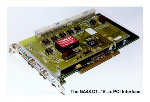
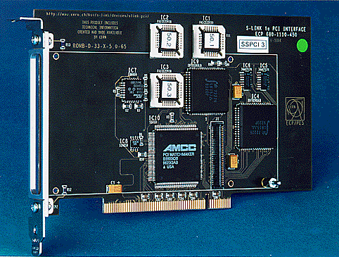
The card sits on top of an S-LINK to PCI interface card. This allows the front panel to reach the slot on the back of the PC.
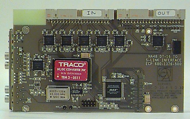
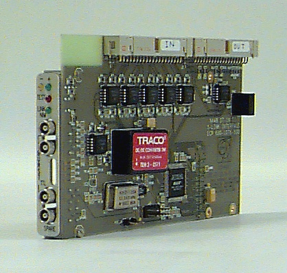
The DT16 connectors are along the top edge. The connector to the S-LINK to PCI card is on the other side. All logic functions are contained in the Altera FPGA at centre-bottom. The row of square chips along the top edge are ECL-TTL converters (DT16 runs at ECL) and the DC/DC convertor provides -5.2V for the ECL chips.
DT16 cables to the connectors are routed through the adjacent slot in
the back of the PC which is free.
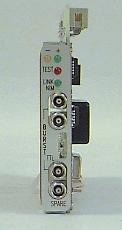
The lemo connectors are to allow end_of_burst signals to be sent directly to the card (normally, these signals are delivered to the PC directly over ethernet). The combination of S-LINK to PCI card and DT2SL interface card occupies two slots on the PCI bus. One slot is occupied by the front-panel and the other is used to route the DT16 cables.