CERN ECP-Division, EDU/DQ Section
Erik van der Bij
7 August 1996
The Simple PMC to S-LINK interface is a PCI Mezzanine Card that is needed to interface S-LINK Link Source Cards (LSCs) in a PMC environment. The interface itself is fully compliant to the PMC as well as the S-LINK specification. However, when the SLINK LSC is plugged onto the SPS, the total height will be larger than allowed by the PMC specification.
The interface was made with simplicity of design in mind. This has consequences for the ease of programming and the maximum transfer rate that the interface can handle. The maximum transfer rate is around 65 MByte/sec with 32-bit SLINK interfaces.
The Simple PMC to S-LINK has Front End Motherboard (FEMB) functionality, is a duplex implementation, with a 33 MHz UCLK frequency, having 5 Volt signal levels and a maximum transfer rate of 65 MByte/sec. In S-LINK terms this is coded as a FEMB-D-33-x-5.0-65.
Furthermore the interface features:
As far as the PMC interface goes it features:
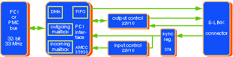
Figure 1 shows a block diagram of the board. The hardware is based on the S5933 PCI controller from the company Applied Micro Circuits Corporation (AMCC). It is this chip that implements the PCI functionality, the DMA interface and access to mailbox registers that control the S-LINK. The S5933 furthermore incorporates several internal registers that provide control and status of the chip itself.
Figure 1: block diagram of the Simple PMC to S-LINK interface
To set up the S-LINK, mailbox register 1 is used. With this register the data width lines, the reset and test lines can be set. Also the value of the control line UCTRL#, which is sent together with each dataword, is set with this register.
To transfer data from the PMC bus to the S-LINK, you can write data into the FIFO port of the S5933. The output control chip will then move the data from the FIFO to the S-LINK when the Link Full Flag line (LFF#) is not asserted. Although the S-LINK specification allows that one extra word may be transferred to the LSC after the LFF# line gets low, this is not done by the Simple PMC to S-LINK interface.
Before writing to the FIFO, you have to check if there is space in the FIFO by reading the Bus Master Control/Status register (MCSR) on the S5933. Another, faster, way of transferring data to the S-LINK is by using the internal DMA. For this the DMA should be enabled by writing to the MCSR. When after that the transfer address and the length of the transfer are set, the DMA will automatically transfer all data into the local FIFO, which then will be transferred to the S-LINK. Whenever the S-LINK is not able to accept the data, the DMA will be suspended. It will continue again when space becomes available in the FIFO. It is possible to let the S5933 generate an interrupt when the DMA is finished.
The input control chip checks if there is any change in the Link Return or LDOWN# Lines from the S-LINK. At startup or if there is a change, it will write the value to mailbox register 4, byte 3. The S5933 can be programmed to generate a PMC interrupt on this event.
The SPS is a standard PMC board and can be mounted with the standard PMC mounting screws. Before mounting it on the motherboard, you should mount the S-LINK Link Source Card with the appropriate screws in the holes foreseen for this purpose.
All accesses to the Simple PMC to S-LINK interface are done via the AMCC S5933 PCI controller chip. It is this chip that needs to be set up for the correct type of PCI accesses with the PCI Configuration Space Registers that are described in the PCI specification and in the AMCC S5933 databook. All accesses to the S-LINK go via the PCI Operation Registers of which the description can be found in the AMCC S5933 databook.
The PCI configuration registers are the standard registers that each PCI compatible card has. Detailed information on the usage of those registers can be found in the PCI Specification and in the AMCC S5933 databook.
Register name : Vendor Identification
Address offset: 00-01h
Boot-load     : 10DCh (CERN)
Attribute     : Read Only (RO)
Size          : 16 bits
Register name : Device Identification
Address offset: 02-03h
Boot-load     : 0010h (Simple PMC to S-LINK interface)
Attribute     : Read Only (RO)
Size          : 16 bits
Register name : PCI Command
Address offset: 04-05h
Boot-load     : 0000h
Attribute     : Read/Write (R/W on 6 bits, Read Only on all others)
Size          : 16 bits
Register name : PCI Status
Address offset: 06-07h
Boot-load     : 0080h
Attribute     : Read Only (RO), Read/Write Clear (R/WC)
Size          : 16 bits
Register name : Revision Identification
Address offset: 08h
Boot-load     : 00h
Attribute     : Read Only (RO)
Size          : 8 bits
Register name : Class Code
Address offset: 09-0Bh
Boot-load     : 028000h     (network controller/
                           other communication device/
                           programming interface 00h)
Attribute     : Read Only (RO)
Size          : 24 bits
Register name : Cache Line Size
Address offset: 0Ch
Boot-load     : 00h
Attribute     : Read Only (RO)
Size          : 8 bits
Register name : Latency Timer
Address offset: 0Dh
Boot-load     : F8h
Attribute     : Read/Write bits 7:3; Read Only bits 2:0
Size          : 8 bits
Register name : Header Type
Address offset: 0Eh
Boot-load     : 00h (Single function device, Format field 0)
Attribute     : Read Only (RO)
Size          : 8 bits
Register name : Built-in Self-test
Address offset: 0Fh
Boot-load     : 00h
Attribute     : D7, D5-0 Read Only, D6 as PCI bus write only
Size          : 8 bits
Register name : Base Address 0
Address offset: 10h
Boot-load     : FFFFFFC0h (64 bytes in memory space)
Attribute     : High bits Read/Write; low bits Read Only
Size          : 32 bits
Register name : Base Address 1-5
Address offset: 14h, 18h, 1Ch, 20h, 24h
Boot-load     : 00000000h (disabled)
Attribute     : High bits Read/Write; low bits Read Only
Size          : 32 bits
Register name : Expansion ROM Base Address
Address offset: 30h
Boot-load     : 00000000h (disabled)
Attribute     : bits 31:11, bit 0 Read/Write; bits 10:1 Read Only
Size          : 32 bits
Register name : Interrupt Line
Address offset: 3Ch
Boot-load     : FFh (unknown)
Attribute     : Read/Write
Size          : 8 bits
Register name : Interrupt Pin
Address offset: 3Dh
Boot-load     : 01h (INTA#)
Attribute     : Read Only (RO)
Size          : 8 bits
Register name : Minimum Grant
Address offset: 3Eh
Boot-load     : 00h (no stringent requirement)
Attribute     : Read Only (RO)
Size          : 8 bits
Register name : Maximum Latency
Address offset: 3Fh
Boot-load     : 00h (no stringent requirement)
Attribute     : Read Only (RO)
Size          : 8 bits
The PCI operation registers are the registers inside the AMCC S5933 chip. All accesses to the S-LINK are done via those registers. Those registers are mapped into the PCI memory space, the base address of them can be found in the PCI configuration space in Base Address Register 0.
The following section describes how the operation registers are used in the interface. Detailed information on the usage of those registers can be found the AMCC S5933 databook.
Register name : Outgoing Mailbox 1
Address offset: 00h
Boot-load     : XXXXXXXXh
Attribute     : Read/Write
Size          : 32 bits
Bit assignment: bit 31-5: not used
                bit 4   : UDW1
                bit 3   : UDW0
                bit 2   : URESET#
                bit 1   : UTEST#
                bit 0   : UCTRL#
Description:
The bits of this register are connected to the corresponding pins of the S-LINK interface. A new value may be written to the Outgoing Mailbox Register at anytime, but the value will only be transferred to the pins of the S-LINK interface if no FIFO transfer is possible. I.e. the FIFO inside the AMCC S5933 chip must be empty before the change is seen. Therefore to be sure a change gets transferred, you have to check the Bus Master Control/Status Register (MCSR) if the PCI to Add-on FIFO is empty before writing the new data. Or, to check if the data is read, you may check the Mailbox Empty/Full Status Register (MBEF) to see if the mailbox register is read by the interface.
Register name : Outgoing Mailbox 2-4
Address offset: 04h, 08h, 0Ch
Boot-load     : XXXXXXXXh
Attribute     : Read/Write
Size          : 32 bits
Description   : those registers have no functionality
Register name : Incoming Mailbox Register 1-3
Address offset: 10h, 14h, 18h
Boot-load     : XXXXXXXXh
Attribute     : Read Only (RO)
Size          : 32 bits
Description   : those registers have no functionality
Register name : Incoming Mailbox Register 4
Address offset: 1Ch
Boot-load     : XXXXXXXXh
Attribute     : Read Only (RO)
Size          : 32 bits
Bit assignment: bit 31-29: read always 0
                bit 28   : LDOWN#
                bit 27   : LRL3
                bit 26   : LRL2
                bit 25   : LRL1
                bit 24   : LRL0
                bit 23-0 : undefined
Description:
The bits in this register are connected to the corresponding lines on the S-LINK connector. If a change that is stable for more than two PCI clock periods (about 60 nsec), occurs on those lines, the new value will be written to the Incoming Mailbox Register 4, byte 3. You may use this event to generate an interrupt by setting up the Interrupt Control/Status Register (INTCSR). You may also check if a new value is written by looking at the Mailbox Empty/Full Status Register (MBEF), bit 31 (note: versions of the board made before August 1996 did not allow the latter).
Note that at power on, the IMB4 register is written with the current
values at that moment. However, the status in the MBEF will not
indicate that the register is written. When you reset the card
via the Bus Master Control/Status Register (MCSR), the IMB4 will
be written with the current values and the MBEF will be updated
correctly.
Register name : FIFO Port
Address offset: 20h
Boot-load     : XXXXXXXXh
Attribute     : Write Only (WO)
Size          : 32 bits
Bit assignment: bit 31-0: UD[31..0]
Description:
If the LSC LFF# line is high, and there is data in the FIFO port, the interface will read the FIFO and transfer the data to the LSC. The UCTRL# line will take the value read from the Outgoing Mailbox Register 1 (OMB1). Beware that a new value of UCTRL# written to the OMB1 only is seen when the FIFO is empty (see the description of OMB1).
Register name : Master Write Address
Address offset: 24h
Boot-load     : 00000000h
Attribute     : Read/Write
Size          : 32 bits
Description   : this register has no functionality
Register name : Master Write Transfer Count
Address offset: 28h
Boot-load     : 00000000h
Attribute     : Read/Write
Size          : 32 bits
Description   : this register has no functionality
Register name : Master Read Address
Address offset: 2Ch
Boot-load     : 00000000h
Attribute     : Read/Write
Size          : 32 bits
Description   : see AMCC S5933 databook
Register name : Master Read Transfer Count
Address offset: 30h
Boot-load     : 00000000h
Attribute     : Read/Write
Size          : 32 bits
Description   : see AMCC S5933 databook
Register name : Mailbox Empty/Full
Address offset: 34h
Boot-load     : 00000000h
Attribute     : Read Only (RO)
Size          : 32 bits
Description   : see AMCC S5933 databook
Register name : Interrupt Control/Status
Address offset:  38h
Boot-load     : 00000000
Attribute     : Read/Write (R/W), Read/Write_One_Clear Only (R/WC)
Size          : 32 bits
Description   : see AMCC S5933 databook
Register name : Bus Master Control/Status
Address offset:  3Ch
Boot-load     : 000000E6h
Attribute     : Read/Write, Read Only, Write Only
Size          : 32 bits
Bit assignment: bit 24    : interface logic reset
                other bits: see AMCC S5933 databook
Description:
Writing a 1 to bit 24 resets the logic on the interface. It does as well pull UDW1, UDW0, URESET#, UTEST# and UCTRL# of the LSC low. For the interface to work, bit 24 must be reset to 0, after which the values for the above mentioned lines are read from the Outgoing Mailbox register 1. Also, Incoming Mailbox 4 will be written and the MBEF register will be updated accordingly.
For the functionality of the other bits of the MCSR, please refer to the AMCC S5933 databook
The previous sections have described the basic functions of the many registers the Simple PMC to S-LINK interface contains. The following sections will give the user some extra information on how to program the device in an optimal way. First it will be described how the PCI interface must be set up. This is followed by sections that explains how to transfer data efficiently and how to handle the return line and link down status changes.
When the host computer where the interface is plugged into, it will have automatically configured the PCI Configuration Registers. Normally there is no need to change any of the values to let the interface operate correctly. You should check the Vendor Identification and Device Identification registers to make sure that the right interface is plugged in.
After that, you should read back the Base Address 0 register to find where the host computer has located the interface in the memory space. The interface will occupy 16 words in total.
The logic on the interface might be reset by writing a 1 to the Add-on Reset bit in the Bus Master Control/Status Register (MCSR). The interface will be ready within 4 PCI clock cycles after the removal of a reset. This reset is not really necessary.
Before any transfer can be done, the Link Source Card lines must be set up. I.e. the value for UDW[1..0], URESET# and UTEST# must be set correctly. This can be done by writing to the Outgoing Mailbox Register 1 (OMB1). At startup the FIFO will be empty, so the newly written value will be seen directly by the LSC. You may check the Mailbox Empty/Full Status Register (MBEF) to check if the value indeed is read by the interface. Normally the interface reads the data within 4 PCI clock cycles (about 120 nsec). If it is not read, it means that a FIFO transfer is in progress. You may have to interrupt any DMA transfers that are in progress by disabling the Read Transfer in the Bus Master Control/Status Register (MCSR).
Before any data may be written into the FIFO, the value of the UCTRL# line has to be set. This can be done by writing to the OMB1 register. Here you have to check if the FIFO is empty, as otherwise the value of UCTRL# will change in another word than you would expect. You might as well check if the newly written value is read by looking at the status in the MBEF register.
For the actual data transfer, you have the option of writing data under processor control or by DMA. For single writes under processor control, you first have to check if there is space available in the FIFO before writing data. Note that a PCI Initiator may not perform burst accesses to the FIFO (see section 10.2.1 of the AMCC databook). For those two reasons, this type of transfer will be relatively slow.
For fast data transfers, you may use the built in DMA engine. This has the advantage that there is no need to check the FIFO status before doing the transfer, as the DMA will stop itself if the FIFO is full and will resume automatically when there is again space available. You may enable the DMA by setting up the Bus Master Control/Status Register (MCSR). After that you only have to write the Master Read Address and Transfer Count registers to let the DMA start. You may set up the interface that it will generate a PMC interrupt when the DMA is finished. Please refer to Chapter 10 of the AMCC databook).
Note that the value of UCTRL# should be the same for the whole DMA transfer. Also you have to wait until the DMA is finished and the FIFO is empty before UCTRL# may be changed.
In case a 16-bit or 8-bit Link Source Card is connected to the board, the interface will only use UD[15..0] or UD[7..0] respectively. This makes that bits UD[31..16] or UD[31..8] are not used. The DMA transfers however, will always be 32-bit transfers, which means that it is not possible to use the DMA if you want to transfer a block of consecutive datawords from the memory.
The current value of the Link Return Lines and the Link Down status from the Link Source Card may be read back in the Incoming Mailbox Register 4, byte 3. You may poll this register, or you might set up the AMCC S5933 to generate an interrupt on a write to this register. The input control logic on the interface will write to this register once at startup and after that only when the Link Return Lines or Link Down lines change and give a stable word for two consecutive PCI clock cycles.
The value of LDOWN# does not interfere with the transfer of data from the FIFO to the Link Source Card.
CERN - High Speed Interconnect
- S-LINK
Erik van der Bij - 7
August 1996