
1. Introduction
The SLITEST is a board in VME form factor that can be used to test S-LINK Link Cards. The card can be used on a desk top with a seperate 5 Volt power supply, or it can used by powering it from a VME crate.
For testing Link Source Cards, the SLITEST has to be used in conjunction with a SLIDAS, while for testing Link Destination Cards a SLIDAD is needed.
Basically the SLITEST is used to use SLIDAS and a SLIDAD cards "upside down". Normally those cards are used to test S-LINK Read-out Motherboards or Front-end Motherboards. As the S-LINK protocol is rather symmetrical on both sides of the link, the rather passive SLITEST board makes that the SLIDAS and SLIDAD can be used to test links. Another application uses the SLITEST in conjunction with a SLIDAD to create an S-LINK data sink.
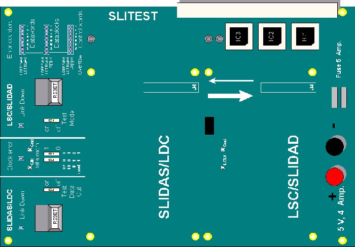
Figure 1: SLITEST Printed Circuit Board
The SLITEST features:
The SLITEST can convert a SLIDAS that has Link Destination Card functionality into having Front-end Motherboard functionality. It can be used as well to convert a SLIDAD that has Link Source Card functionality into a card that has Read-out Motherboard functionality. Therefore with a pair of SLITESTS, a SLIDAS and a SLIDAD, an S-LINK can easily be tested (see figure 2).
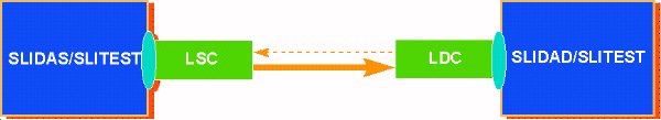
Figure 2: S-LINK test setup using SLITEST
The functionality of the SLITEST is easily accomplished as the S-LINK signals at the LSC and the LDC side are highly symmetrical. E.g. the timing and functionality of the clock, write enable and data lines are the same on both sides, while they are inputs on the LSC and outputs of the LDC. This makes that the signals of the SLIDAS can directly be connnected to the LDC, and the LDC signals can directly be connected to the SLIDAS. On the SLITEST this is done for the signals:
The SLITEST generates some signals itself as they are inputs on both the LSC and LDC side:
The LDOWN# signals are outputs on both the LSC and LDC. Therefore they are shown on LEDs.
When the SLITEST is used to connect an LDC to a SLIDAD, the LDERR# line is giving out the error information. The SLITEST has counters for the different types of errors, which are:
As the load on the clock from the LDC card is relatively high because of the error counters, a Phase Locked Loop circuit is included on the SLITEST. This has no influence on the timing, but it makes that the LCLK frequency has to be between 20 MHz and 35 MHz according to the specifications of the PLL chip. In practice the boards work between 10 MHz and 40 MHz. If the PLL is not locking, the Clock Error LED will light up. If a board needs to be tested at low frequencies (under 10 MHz), the PLL chip could be removed in which case the pads for pins 7, 14, 16, 21 and 23 should be connected together.
For connecting a Link Source Card, plug the Link Source Card into the location marked LSC/SLIDAD. In that case a SLIDAS should be mounted at the location marked SLIDAS/LDC. The keying pins should prevent inserting the boards wrongly.
If a Link Destination Card has to be tested, insert it in the location marked SLIDAS/LDC. In that case a SLIDAD should be mounted at the location marked LSC/SLIDAD. This is shown in figure 3.
To prevent contact problems or mechanical stress on the connector, always mount all four screws that hold the cards, even when doing quick tests.
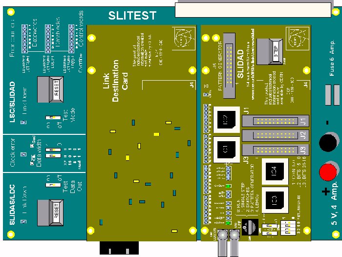
Figure 3: SLITEST with LDC and SLIDAD mounted
The SLITEST can be powered by either plugging it in a standard 6U VME crate where it will take the 5 Volt from pins B1, B13 and B32 of the P2 connector. Ground is coming from pins B2, B12, B22 and B31. Another option is to power it with the two banana plugs on the board. The board is protected by 5 Amp fuses. A SLITEST populated with two cards is typically drawing two to three Amp.
Reset button BP1 is used to reset the SLIDAS/LDC site. It uses the clock of the SLIDAS/LDC to generate the reset protocol (URESET#/LDOWN# handshake). Therefore if there is no clock from the SLIDAS or LDC, it will not work. LD1 shows the state of the LDOWN# flag. If LDOWN# is active (0), the LED will be lit.
The Test Data Out switch SW1 is used to set the UTDO# level. In position ON, UTDO# is active (0), in position OFF, UTDO# is inactive (1). Note that a change in UTDO# should only be taken into account by the LDC or SLIDAS after a reset is given.
If the Clock Error LED (LD2) is lit, the Phase Locked Loop on the SLITEST is not locked. LCLK from the SLIDAS/LDC slot has to be between 20 MHz and 35 MHz according to the specifications of the PLL chip. In practice the boards work between 10 MHz and 40 MHz. That the LED is not on, does not guarantee the PLL is locked, notably for low frequencies this can be true.
The Data Width switches set the values of UDW[1..0] on both sites. Note that a Link Card will sample the value of those lines only after a reset cycle.
The Test Mode switch SW4 sets the value of UTEST# of the LSC/SLIDAD slot. In the ON position, UTEST# is active (0).
Reset button BP2 is used to reset the LSC/SLIDAD site. It uses the clock of the SLIDAS/LDC to generate the reset protocol (URESET#/LDOWN# handshake), therefore if there is no clock from the SLIDAS or LDC, it will not work. LD3 shows the state of the LDOWN# flag of the LSC/SLIDAD. If LDOWN# is active (0), the LED will be lit. The reset button will also reset the error counters.
The error counter LEDs count the different types of errors that a Link Destination Card can show. These are various combinations of the LCTRL#, LDERR# and LD[1..0] lines:
The counters can count up to 127 errors. If more are received, the overflow LED will light up.
There are two test points for the clock signals. LCLK is connected to LCLK signal from the SLIDAS/LDC slot. CLK-bar is connected to an output of the Phase Lock Loop chip and should give out an inverted LCLK.
The following signals have a single load when both slots are used:
The following signals have a load of 4 when both slots are used:
CERN - High Speed Interconnect
- S-LINK
Erik van der Bij - 7 April
1997