The block diagram of the HS-Link evaluation board is shown in figure 4. A T8 microcontroller is used to initialise and monitor the status of the Bullit chips and of the RCube switch. There are FIFO buffers connected directly to each Bullit so that data can be passed at the full link rate through the parallel port of these devices.
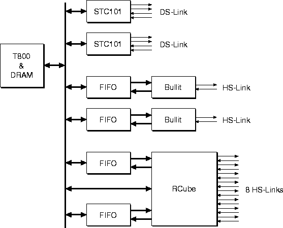
Figure 4: Block Diagram of the HS-Link Evaluation Board
The Bullit chips act as HS-Link data sources and sinks. Before a test begins, the processor loads the data to be transmitted into the associated FIFO buffer. After the transmission has finished the processor can then read the data from the FIFOs to check if any errors have occurred. There are different modes of operation: half-duplex and full-duplex burst data transmission, ``ping-pong'', i.e. transmission of data from the FIFO on one Bullit into the other one and back again, and continuous wrap-around, where data is circulated bidirectionally between the two Bullit devices.
All the HS-Links connections are made using micro coaxial cables. This allows for direct connections between Bullit chips or via the RCube switch. By looping the links of the RCube switch back onto itself and setting up the routing tables appropriately, data can be sent through all the links of the switch concurrently, even though there are only two data sources.
The STC101 devices have been incorporated to develop support for a DS-Link control network for configuration, control and monitoring of a network of RCube switches, as described in section 5 below.