

S-LINK News 1998
LynxOS driver ported to Motorola VME platform
13 November 1998. Juanba
Romance from IFIC/Valencia is writing software for the TileCal
ROD. He has ported to the Motorola platform the LynxOS
drivers that were written by the DAQ
Prototype -1 project for the CES platform.
DAQ Event format
9 November 1998. It's one thing to define the link type to use in
your data acquisition system, but it's another thing to decide on the way
you are going to send your data over it. Of course also here a standard
is needed. The first step in defining the final ATLAS event format is made
in the document "The
event format in the ATLAS DAQ/EF prototype -1" (ATL-DAQ-98-129).
This note presents the event format to be used in the ATLAS DAQ/EF prototype
-1 and it covers the format of the data input to the Read-Out Crates from
the Read-Out drivers and up to the input of the Event Filter.
Integrated FCS-LINK LDC with PMC logic
4 November 1998. Currently all S-LINK links are implemented as daughtercards
of the size of a PMC card. To reduce cost, it is foreseen that in final
applications the link logic may be integrated on the front-end motherboard
or on the read-out motherboard. As currently most designs are prototypes
and as link technologies are still rapidly changing and are becoming cheaper,
it is still too early to integrate the link logic on the motherboards.
However, we have to learn already now if any difficulties will arise
if S-LINK logic is integrated with other logic. One may think of problems
of the co-existence of gigabit signals on boards with other frequencies,
EMC, noise on power supplies etc. To get experience with this, we have
set up a project with Wieslaw Iwanski of the Institute of Nuclear Physics
in Krakow who will integrate Fibre Channel Link Destination Card logic
with S-LINK to PMC card logic. Once the boards are working, they may be
used in testbeams where VME processor boards are used to read out detectors
with FCS-LINK2 cards. A design review of the schematics has been made and
the PCB is being designed now. A review of the PCB layout will be done
before five boards will be produced.
Workshop on Electronics for LHC Experiments (LEB98):
"S-LINK: A Prototype of the ATLAS Read-out Link"
18 September 1998. S-LINK will be presented at the LEB98
workshop in the paper called "S-LINK:
A Prototype of the ATLAS Read-out Link". (1.5 MB .ps).
For those who would like to read it like some people read detectives:
Abstract
The ATLAS data acquisition system needs over 1500 read-out links between
the read-out drivers and the read-out buffers. As it is too early to define
the physical layer of those links, the S-LINK specification has been written.
It defines a media independent 32-bit synchronous FIFO-like interface for
both the sender and receiver side of a link. S-LINKs can send control and
data words, can detect link errors and have a self-test mode. Fibre-optic
gigabit versions of S-LINK are used by various ATLAS detectors as prototype
read-out link and also as trigger information distribution link.
Conclusions
The S-LINK specification describes an easy-to-use datalink which relieves
read-out designers from the task of designing high frequency transmission
circuits with error detection capabilities. Links, interfaces and test
tools have been designed and are commercially available. S-LINK has been
used already in several applications within ATLAS, other experiments and
also outside high energy physics. Considerable knowledge and experience
with the links, test tools and software has been built up, while also the
robustness of the cards and tools has been proven. Ongoing efforts are
being made to reduce the price of the links, to make a radiation tolerant
version and to allow easier integration into large scale systems. Furthermore
extensive support is given to projects inside and outside ATLAS that
want to incorporate S-LINK.
 MEGACAM: S-LINK looking at the stars
18 September 1998. S-LINK might be used in the readout system of
the MEGACAM astronomical camera. MEGACAM is the next generation wide-field
camera to be used at the prime focus of the 3.6m CFHT telescope. This instrument,
which will cover a full 1 square degree, is designed around a mosaic of
36 to 40 2Kx4K CCDs. Such a large detector requires new approaches for
the hardware as well as the software, and will have major impacts on the
telescope structure, optics and operations. MEGACAM will start operating
in the year 2001.The camera will be designed and built at DAPNIA (Department
d'Astrophysique, de Physique des Particules, de Physique Nucleaire et d'Instrumentation
Associee), which is a division of the CEA (French Atomic Energy Commission).
The CFHT is the first telescope built on the Mauna Kea. Mauna Kea is
the highest volcano of Hawaii (4200m). It is always above the clouds, far
away from civilisation and is seen as the world's best astronomical site.
The total image containing 320 million pixels is 640 MByte. The MEGACAM
readout requires two to four gigabit links for a readout time of less
than 20 seconds. The CCDs are connected to a SHARC DSP. SHARC to S-LINK
logic will move the data to Motorola MVME processor boards running VxWorks
with a commercially available S-LINK to
PMC interface mounted on it
Simplex G-LINK Link Destination being designed
17 September 1998. We have ordered five printed circuit boards of
the Simplex G-LINK Link Destination Card
(G-LDC). The G-LDC is an S-LINK compliant LDC which is based on the
Hewlett Packard 5 Volt G-LINK receiver HDMP-1024. The G-LDC can work in
conjunction with transmitter boards that use the corresponding transmitter
HDMP-1022 or other chips that follow the G-LINK protocol.
The optical input of the card uses the Finisar FRM-8510 850 nm receiver
module while a seperate A/D converter measures the optical power level
of the light received. For laboratory tests, also LEMO connectors may be
mounted to access directly the G-LINK serial inputs. For even more flexibility
the Finisar module or LEMO connectors may be mounted on either side of
the card. This G-LDC is another example of the independence of S-LINK to
the physical link components used. Once testing has finished, it is planned
to make the cards available via a commercial company.
NIKHEF has written a Windows/NT driver for S-LINK
9 September 1998. A Windows
NT driver for the PCI to S-LINK interface
and the S-LINK to PCI interface has
been written at NIKHEF. Also performance
measurements have been made, which show that a bandwidth of around 41 MByte/sec
out of the theoretical 65 MByte/sec can be reached with the PCI to S-LINK
interface. The S-LINK to PCI interface has a much higher rate (NA48
has measured 117 MByte/sec), but no seperate measurements have been done
with the NT destination driver yet.The NT driver is available from NIKHEF
on request.
NA48 has taken 60TByte (60 000 Gbyte) of physics events over S-LINK to
PCI interface
 21
August 1998. The NA48 Experiment at CERN has installed a
PC farm for data acquisition and event-building in the the 1998 run
period. Each subdetector in the experiment is connected to a SubDetector
PC (SDPC) and dumps all its data into this PC during the SPS (Super Proton
Synchrotron) burst (2.5s every 14.4s). The subdetectors front-end
link is called DT16 (an ECL-type parallel link). The DT2SL interface converts
the DT16 into an S-LINK compliant LDC. This interface is then plugged onto
commercially available S-LINK to PCI cards
to interface to the PCI bus on the SDPC.
21
August 1998. The NA48 Experiment at CERN has installed a
PC farm for data acquisition and event-building in the the 1998 run
period. Each subdetector in the experiment is connected to a SubDetector
PC (SDPC) and dumps all its data into this PC during the SPS (Super Proton
Synchrotron) burst (2.5s every 14.4s). The subdetectors front-end
link is called DT16 (an ECL-type parallel link). The DT2SL interface converts
the DT16 into an S-LINK compliant LDC. This interface is then plugged onto
commercially available S-LINK to PCI cards
to interface to the PCI bus on the SDPC.
After delivery of the switch and the PCs it took about a month to move
the hardware in place, connect the PCs to the subdetectors, install the
operating system and do the first-level debugging of the already prepared
event building software. The farm is running smoothly and by now more than
60TByte (60 000 Gbyte) of physics events have been read out over the S-LINK
to PCI interfaces and sent to the computer centre's tape robots.
How to test S-LINK equipment?
6 August 1998. SLIDAS, SLIDAD,
SLITEST, SLIBOX,
microSLATE... One of
the most difficult parts of S-LINK is to understand exactly what test tools
you can use to do what. On the other hand it is also the power of S-LINK
that we have all tools available you ever may need. To get an impression
on what is possible, have a look at the slideshow
"S-LINK Test Tools". Of course if you have any questions, or
would like to see or even borrow some tools, don't hesitate to contact
anyone of the S-LINK team.
ROB-in with i960 processor delivered to DAQ Prototype-1
5 August 1998. The PCI version of the Royal
Holloway ROB-in (Read-out Buffer input), which is based on an Intel
i960 processor is working. One board has been delivered to the CERN DAQ
Prototype-1 project. The ROB-in has been tested there with the help
of Gordon Crone from the University College of London who also wrote the
firmware of the board. The DAQ Prototype-1 project has defined and implemented
an Application Interface for the ROB-in.
S-LINK will be presented at the Workshop on Electronics for LHC Experiments
(LEB98)
5 August 1998. The purpose of the LEB
workshop is to identify areas and encourage common efforts for development
of electronics within and between the different LHC experiments, and to
promote cross fertilisation in the engineering and physics communities
involved in the LHC activities. S-LINK is a good example of a common effort
as it is and will be used by many different detectors and readout systems.
You may read the summary of the presentation "S-LINK:
a Prototype of the ATLAS Read-out Link" that will be given at the
workshop.
S2P2: an S-LINK to VME P2 adapter
24 June 1998. The S-LINK to P2 (S2P2)
adapter is a VME board that can carry an S-LINK Link Source Card or
Link Destination Card. The S2P2 is a passive board, which connects all
S-LINK signals to rows A and C of the VME P2 connector. With a short cable
or backplane plug connected to the VME backplane, the S-LINK signals can
be fed into the slot next to the S2P2, where they can be brought up to
the JN14 PMC connector. The S2P2 is powered via the P2 connector. PMC cards
like the MFCC
from CES and the PMC version of the ATLAS
Royal Holloway ROB-in can use the S2P2 to provide robust connectivity
to S-LINK. The PCB of the S2P2 has been designed and it will be manufactured
in July.
TileCal readout groups buy S-LINK equipment
7 April 1998. It is planned to transmit data from the ATLAS Tile
Calorimeter front-end electronics to the readout driver (ROD) modules
by optical S-LINK. The front-end electronics is housed in 256 3-m-long
drawers located on the detector. Chicago and Stockholm are preparing the
front-end electronics and Valencia the RODs.
The first demonstration of the system using Fibre Channel S-LINK will
take place in the CERN H8 test beam in July 1998. A complete set of S-LINK
test tools, an fc
S-LINK and an S-LINK
to PMC interface have been purchased from commercial vendors by Chicago
and Stockholm for development and testing in their home laboratories. In
this first demonstration a CES
8062 VME-processor module will host the PMC card as part of the RD-13
DAQ system. Vicente Gonzalez is in contact with David Francis from the
Prototype-1 DAQ project for
details on sending data from S-LINK into a VME-based system.
New user's guide for SLIDAD
17 March 1998. The SLIDAD is a stand-alone device that connects
to the S-LINK connector of a Front-end Motherboard (FEMB). You can use
it to test the hardware of a FEMB at its S-LINK interface without having
to set up a real S-LINK with software on the receiving side.
You plug the SLIDAD instead of a Link Source Card on the FEMB, so it
will show the data that is sent by the FEMB. You can see directly the data
you send on LED's and you may connect a logic state analyser to the three
20-pin connectors. You may also set the values of the return lines. With
the single-step mode you can even receive and check the data on a word-by-word
basis. Advanced set-up and trigger files for HP16500 Logic State analysers
are available.
This handy device is commercially available since more than a year.
The web page for it and it's user's
guide are renewed.
TileCal will order S-LINK test tools and PMC interface for June testbeam
9 March 1998. The ATLAS
TileCal plans to take data over S-LINK in the testbeam of June. Alfonso
Rios has visited the CERN S-LINK laboratory to see what equipment is needed
and what software is available. The conclusion is that they need a Fibre
Channel version of S-LINK and an S-LINK
to PMC interface. The TileCal read-out is in a VME environment and
they will use a CES RIO2 for the connectivity to VME. Another possibility
would have been to use the VMETRO MIDAS, but currently no software for
this platform is available and also price-wise the MIDAS does not appear
a viable solution.
To allow the software development and hardware development go on as
long as possible in parallel, a complete set of test tools will be ordered.
With the SLIDAD the design of the Read-Out
Driver can be tested with just a logic state analyzer, and with the SLIDAS
data can be generated to test the software without needing the detector
in place. As driver for LynxOS, the driver from the DAQ/Event
Filter Prototype -1 Project will be used.
Olivetti and Oracle Research Laboratories use S-LINK in CPCI environment
6 March 1998. ORL has got the
first prototype of the 'StrongTile' network computer working. In this configuration
a Linux host workstation communicates with the StrongTile (a framestore
card for LCD panels) over S-LINK using the Remote Frame Buffer (RFB)
protocol used by the Virtual Network
Computer (VNC). Currently they use commercially available fcS-LINK
cards in combination with PCI
to S-LINK interfaces. As the StrongTile network computer is based on
Compact PCI (CPCI), a CPCI to PCI adapter is used. ORL plans to build a
native CPCI to S-LINK interface based on CERN's PCI to S-LINK design.
Some pictures
of the StrongTile with S-LINK in action are available. For more information,
take a look at ORL's Terminal
Remoting over S-LINK web page.
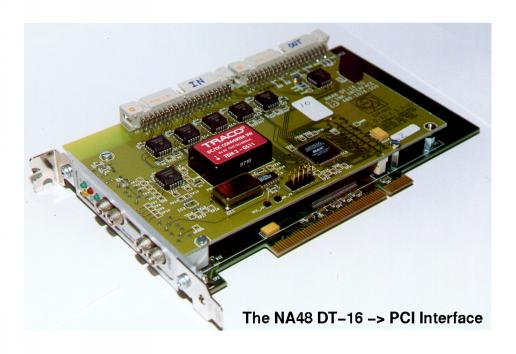
 15
NA48 DT-16 to S-LINK interfaces produced
15
NA48 DT-16 to S-LINK interfaces produced
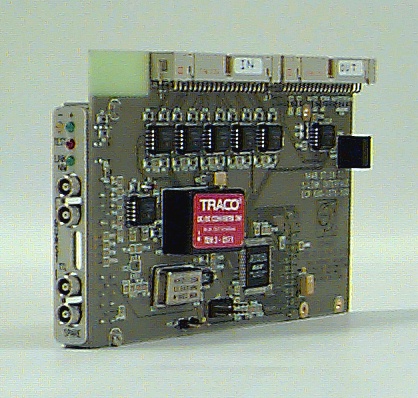
6 March 1998. NA48 has built and tested fifteen DT2SL interfaces.
The DT2SL interface
converts the DT16 (an ECL-type parallel link coming from the front-end
electronics) into an S-LINK compliant LDC. This interface is then plugged
onto an existing S-LINK to PCI card to interface to the PCI bus on the
SDPC. The advantage of this approach is that the DT16 to S-LINK conversion
is relatively simple - much simpler than building an interface from DT16
to PCI directly. This also allowed NA48 to take advantage of the commercially
available S-LINK to PCI card and of the considerable amount of S-LINK experience
and test hardware which is available.
NA48 will now start to integrate those cards into fifteen PC's, which
all run Linux. The drivers for this have already extensively been tested.
Fibre Channel S-LINK Cards available from CERNTECH
3 March 1998. The Fibre Channel S-LINK cards are now available directly
from the designers. They have set up the company called CERNTECH,
based in Hungary. Detailed
information, including pricing, is also available on their web site.
S-LINK to PMC performance report on the web
3 March 1998. In the framework of the ATLAS DAQ Prototype -1 work,
performance measurements of the S-LINK to PMC interface have been made.
As datasource the SLATE and a SLIDAS have been used. As software two applications
have been written: a simple destination and a simple Read-out Buffer (ROB)
program. DMA performances of 72 MByte/sec have been measured with a CES
RIO2. With a simple destination program transfer rates of 49.2 MByte/sec
and a transfer frequency 48 KHz have been measured for data packets of
1084 bytes. The frequency goes up to 120 KHz for the transfer of packets
of 64 bytes. The full report, entitled S-LINK performance measurements
in the environment of ATLAS DAQ/EF prototype -1 is available on the
web (Postscript
340 KB).
Fibre Channel S-LINK: cheaper by integrating optical module
26 January 1998. The Fibre
Channel S-LINK, also known as the FCS-LINK, has been working
already since September 1996. That board uses a GigaLink
Module (GLM), which is a plug-in module doing the serialisation and
electrical-to-optical conversion. With a price of almost $400, this GLM
is the most expensive part of the board. To reduce the price, and also
to jump on the Gigabit Ethernet bandwagon, where we expect to find cheaper
components, we have chosen to integrate the logic which normally is found
on the GLM (electrical transceiver and optical transceiver) directly onto
the S-LINK card. In this case the optical transceiver with a price in the
order of $200 becomes the most expensive part. However, in many cases,
such as in laboratory setups, there is no need for a transmission over
optical media. Therefore we have made the possibility to mount a Gigabit
Ethernet electrical connector instead of the optical transceiver. This
will reduce the component price by another $160, which will be reflected
by a few factors in the sales price.
With the extra options of being able to mount the connectors on the
top side (for PMC applications) or on the bottom side (for PCI applications),
the new board can be used in most applications. As has always been the
aim of S-LINK, the users will not have to change anything on their
boards to use this new, cheaper card. The PCB
of this new FCS-LINK is expected to return from fabrication
by the end of February.
COMPASS S-LINK to PCI interface underway
 26
January 1998. COMPASS will
use S-LINK in the DAQ system. To handle the spill mechanism, they are
designing a Read-Out Motherboard having a buffer of up to 64 Megabytes
that can receive all data from one spill before reading it out much slower
over a PMC or PCI bus. This way one PC can handle several Read-out Motherboards.
26
January 1998. COMPASS will
use S-LINK in the DAQ system. To handle the spill mechanism, they are
designing a Read-Out Motherboard having a buffer of up to 64 Megabytes
that can receive all data from one spill before reading it out much slower
over a PMC or PCI bus. This way one PC can handle several Read-out Motherboards.
A PCI card is being built that has the 64 MByte of SIMM memory and the
PCI interface integrated. The design is basically an S-LINK FIFO connected
to the S-LINK to PCI interface that has been in production since 1997.
The S-LINK Link Destination Card can be plugged on top of this card. The
two boards together will take up only one PCI slot, just like the S-LINK
to PCI interface. The PCB is ready; it is expected that testing of
the cards will start in February.
Old S-LINK News
CERN - High Speed Interconnect
- S-LINK
Erik van der Bij - 13 November
1998